TN5335 Ver la hoja de datos (PDF) - Supertex Inc
Número de pieza
componentes Descripción
Fabricante
TN5335 Datasheet PDF : 2 Pages
| |||
Thermal Characteristics
Package
ID (continuous)*
ID (pulsed)
Power Dissipation
@ TA = 25°C
θjc
°C/W
TO-236AB
110mA
800mA
0.36W
200
TO-243AA
230mA
1.3A
1.6W†
15
* ID (continuous) is limited by max rated Tj.
† Mounted on FR5 board, 25mm x 25mm x 1.57mm. Significant PD increase possible on ceramic substrate.
θja
°C/W
350
78†
Electrical Characteristics (@ 25°C unless otherwise specified)
IDR*
110mA
230mA
TN5335
IDRM
800mA
1.3A
Symbol
BVDSS
VGS(th)
∆VGS(th)
IGSS
IDSS
Parameter
Drain-to-Source Breakdown Voltage
Gate Threshold Voltage
Change in VGS(th) with Temperature
Gate Body Leakage
Zero Gate Voltage Drain Current
Min Typ Max Unit
350
V
0.6
2.0
V
-4.5 mV/°C
100
nA
1.0
µA
10
µA
1.0 mA
ID(ON)
RDS(ON)
ON-State Drain Current
Static Drain-to Source
On-State Resistance
5.0
300
750
15
15
15
∆RDS(ON) Change in RDS(ON) with Temperature
1.0
GFS
Forward Transconductance
125
CISS
Input Capacitance
110
COSS
Common Source Output Capacitance
60
CRSS
Reverse Transfer Capacitance
22
td(ON)
Turn-ON Delay Time
20
tr
Rise Time
15
td(OFF)
Turn-OFF Delay Time
25
tf
Fall Time
25
VSD
Diode Forward Voltage Drop
1.8
trr
Reverse Recovery Time
800
Notes:
1. All D.C. parameters 100% tested at 25°C unless otherwise stated. (Pulse test: 300µs pulse, 2% duty cycle.)
2. All A.C. parameters sample tested.
nA
mA
Ω
%/°C
m
pF
ns
V
ns
Conditions
VGS = 0V, ID = 100µA
VGS = VDS, ID= 1mA
VGS = VDS, ID= 1mA
VGS = ± 20V, VDS = 0V
VGS = 0V, VDS = 100V
VGS = 0V, VDS = Max Rating
VGS = 0V, VDS = 0.8 Max Rating
TA = 125°C
VGS = 0V, VDS = 330V
VGS = 4.5V, VDS = 25V
VGS = 10V, VDS = 25V
VGS = 3.0V, ID = 20mA
VGS = 4.5V, ID = 150mA
VGS = 10V, ID = 200mA
VGS = 4.5V, ID = 150mA
VDS = 25V, ID = 200mA
VGS = 0V, VDS = 25V
f = 1Mhz
VDD = 25V,
ID = 150mA,
RGEN = 25Ω
VGS = 0V, ISD = 200mA
VGS = 0V, ISD = 200mA
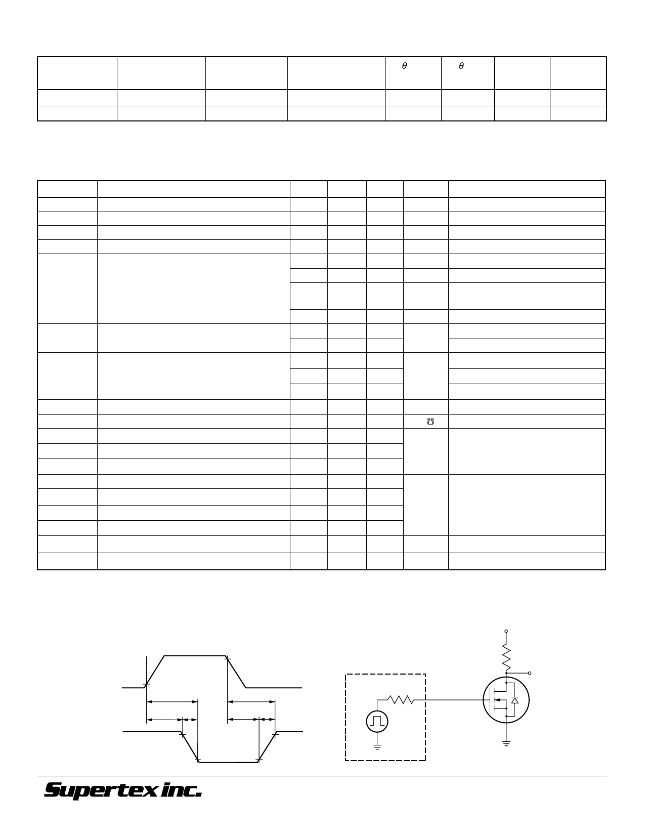
Switching Waveforms and Test Circuit
10V
INPUT
0V
10%
VDD
OUTPUT
0V
t(ON)
td(ON)
tr
10%
90%
90%
t(OFF)
td(OFF)
tF
10%
90%
©2001 Supertex Inc. All rights reserved. Unauthorized use or reproduction prohibited.
2
PULSE
GENERATOR
Rgen
INPUT
VDD
RL
OUTPUT
D.U.T.
11/12/01
1235 Bordeaux Drive, Sunnyvale, CA 94089
TEL: (408) 744-0100 • FAX: (408) 222-4895
www.supertex.com
Share Link: 