CMPWR330 Ver la hoja de datos (PDF) - California Micro Devices => Onsemi
Número de pieza
componentes Descripción
Fabricante
CMPWR330 Datasheet PDF : 8 Pages
| |||
CALIFORNIA MICRO DEVICES
CMPWR330
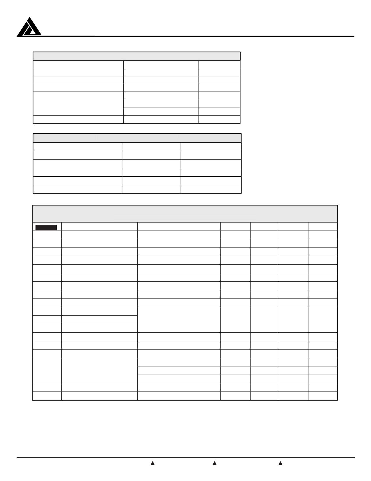
ABSOLUTE MAXIMUM RATINGS
Parameter
Rating
ESD Protection (HBM)
2000
VCC, VSBY Input Voltage
6.0, GND –0.5
VAUX Input Voltage
4.0, GND –0.5
Temperature: Storage
–40 to 150
Operating Ambient
0 to 70
Operating Junction
0 to 125
Power Dissipation: (Note 1)
Internally Limited
OPERATING CONDITIONS
Parameter
Range
VCC , VSBY
VAUX
Temperature (Ambient)
5 ± 0.25
3.3 ± 0.3
0 to 70
Load Current
0 to 400
CEXT
10 ± 20%
Unit
V
V
V
°C
°C
°C
W
Unit
V
V
°C
mA
µF
ELECTRICAL OPERATING CHARACTERISTICS
(over operating conditions unless specified otherwise)
Symbol
Parameter
Conditions
MIN
TYP
MAX
UNIT
VOUT
Regulator Output Voltage
0mA < ILOAD < 400mA
3.135
3.30
3.465
V
ILIM
Regulator Current Limit
500
mA
IS/C
Short Circuit Current
VCC/SBY = 5V, Vout = 0V
150
mA
VR LOAD Load Regulation
VCC = 5V, ILOAD = 5 to 400mA
20
mV
VR LINE Line Regulation
VCC = 4.5V to 5.5V, ILOAD = 5mA
2
mV
VCCSEL VCC Select Voltage
VSBY or VAUX present
4.40
4.60
V
VCCDES VCC Deselect Voltage
VSBY or VAUX present
4.00
4.20
V
VHYST
RSW
Hysteresis Voltage (Note 2)
VAUX Switch Resistance
VSBY or VAUX present
0.20
V
0.25
0.4
Ω
IRCC
IRSBY
IRAUX
VCC Reverse Leakage
VSBY Reverse Leakage
VAUX Reverse Leakage
One supply input taken to
ground while the others remain
at nominal voltage
5
100
µA
ICC
VCC Supply Current
VCC > VCCSEL, ILOAD = 0mA
0.8
1.5
mA
ISBY
VSBY Supply Current
VCC < VCCDES, ILOAD = 0mA
0.8
1.5
mA
IAUX
VAUX Supply Current
VAUX is selected, ILOAD = 0mA
0.2
0.30
mA
IGND
Ground Current
VAUX is selected, (vCC/SBY = 0V)
0.2
0.30
mA
VCC/SBY = 5V, ILOAD = 0mA
0.8
1.5
mA
TDISABLE Shutdown Temperature
THYST
Thermal Hysteresis
VCC/SBY = 5V, ILOAD = 400mA
1.0
2.0
mA
160
°C
20
°C
Note 1: At rated load, the power dissipation will be 0.68W (1.7V x 0.4A). Under these conditions, (in a 70°C ambient), the thermal
resistance from junction to ambient (θJA) must not exceed 80°C/W. This is typically achieved with 2 square inches of copper printed
circuit board area connected to the GND pins for heat spreading, or equivalent.
Note 2: The disturbance on VCC during supply changeover should be kept below the hysteresis voltage to prevent any chatter. The source
resistance on the VCC supply should be kept to less than 0.3Ω to ensure precise switching.
©2001 California Micro Devices Corp. All rights reserved. Smart OR™ is a trademark of California Micro Devices.
215 Topaz Street, Milpitas, California 95035 Tel: (408) 263-3214
2
Fax: (408) 263-7846
www.calmicro.com
3/6/2001
Share Link: 