6521CBZ Ver la hoja de datos (PDF) - Intersil
Número de pieza
componentes Descripción
Fabricante
6521CBZ Datasheet PDF : 13 Pages
| |||
HIP6521
equally large amounts of noise. The critical small signal
components are those connected to sensitive nodes or
those supplying critical bypass current.
The power components and the controller IC should be
placed first. Locate the input capacitors, especially the
high-frequency ceramic decoupling capacitors, close to the
power switches. Locate the output inductor and output
capacitors between the MOSFETs and the load. Locate the
PWM controller close to the MOSFETs.
+5VIN
LIN
+
CIN
VOUT2
+
COUT2
+12V
CVCC
VCC GND
OCSET
COCSET
ROCSET
UGATE
PHASE
Q1
LOUT
VOUT1
DRIVE2
Q3
LGATE
Q2
COUT1+
CR1
VOUT3
+
COUT3
Q4
HIP6521
VOUT4
DRIVE3 DRIVE4
+
COUT4
PGND
Q5
+3.3VIN
KEY
ISLAND ON POWER PLANE LAYER
ISLAND ON CIRCUIT OR POWER PLANE LAYER
VIA CONNECTION TO GROUND PLANE
FIGURE 5. PRINTED CIRCUIT BOARD POWER PLANES AND
ISLANDS
The critical small signal components include the bypass
capacitor for VCC and the feedback resistors. Locate these
components close to their connecting pins on the control IC.
A multi-layer printed circuit board is recommended.
Figure 5 shows the connections of the critical components
in the converter. Note that the capacitors CIN and COUT
each represent numerous physical capacitors. Dedicate
one solid layer for a ground plane and make all critical
component ground connections with vias to this layer.
Dedicate another solid layer as a power plane and break
this plane into smaller islands of common voltage levels.
The power plane should support the input power and
output power nodes. Use copper filled polygons on the top
and bottom circuit layers for the PHASE nodes, but do not
unnecessarily oversize these particular islands. Since the
PHASE nodes are subjected to very high dV/dt voltages,
the stray capacitor formed between these islands and the
surrounding circuitry will tend to couple switching noise.
Use the remaining printed circuit layers for small signal
wiring. The wiring traces from the control IC to the
MOSFET gate and source should be sized to carry 2A peak
currents.
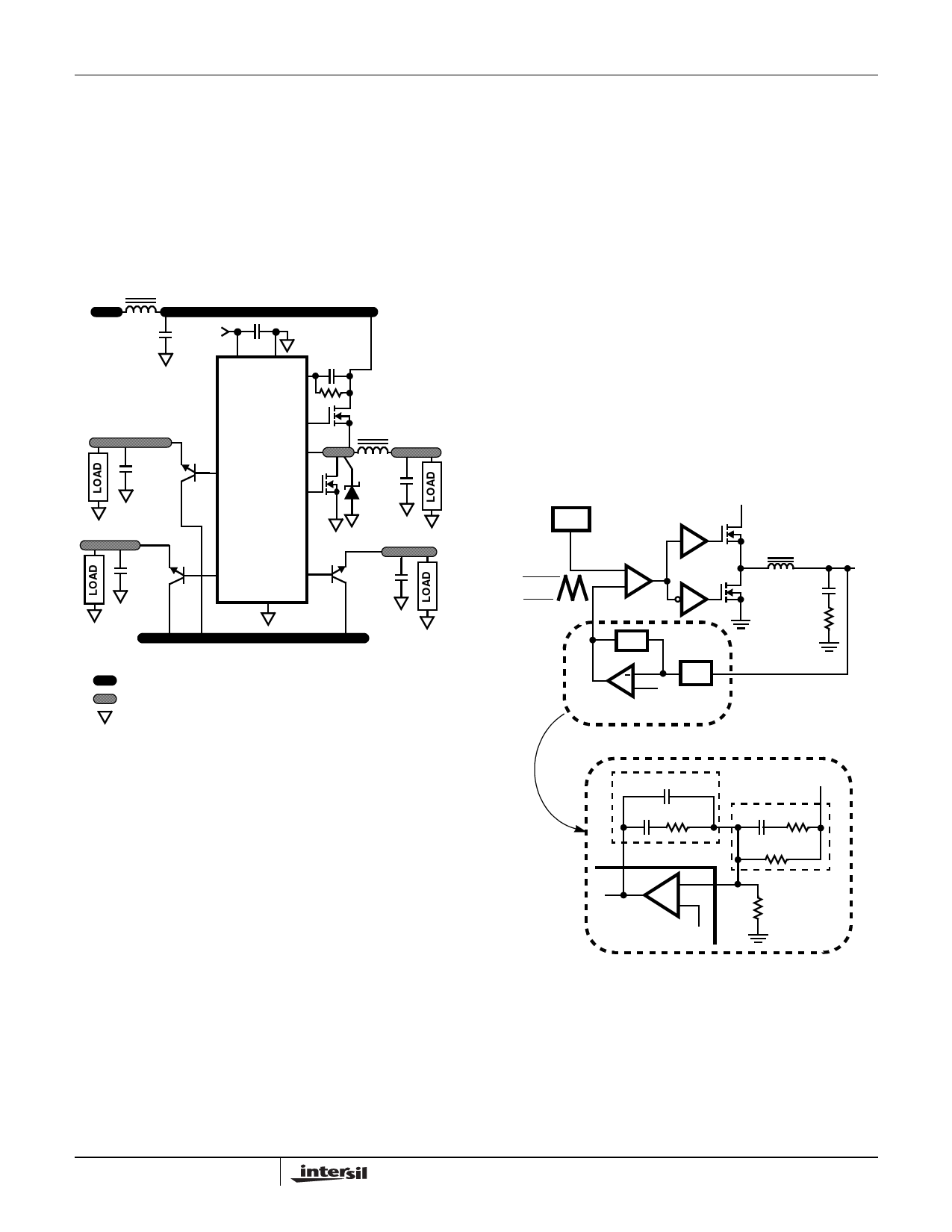
PWM Controller Feedback Compensation
The PWM controller uses voltage-mode control for output
regulation. This section highlights the design consideration
for a PWM voltage-mode controller. Apply the methods and
considerations only to the PWM controller.
Figure 6 highlights the voltage-mode control loop for a
synchronous-rectified buck converter. The output voltage
(VOUT) is regulated to the Reference voltage level, 0.8V.
The error amplifier (Error Amp) output (VE/A) is compared
with the oscillator (OSC) triangular wave to provide a
pulse-width modulated (PWM) wave with an amplitude of
VIN at the PHASE node. The PWM wave is smoothed by the
output filter (LO and CO).
OSC
∆ VOSC
VIN
DRIVER1
PWM
COMP
-
+
ZFB
SYNC
DRIVER
LO
PHASE
VOUT
CO +
ESR
(PARASITIC)
VE/A
+
ERROR
AMP
ZIN
0.8V
DETAILED COMPENSATION COMPONENTS
C2
C1 R2
ZFB
VOUT
ZIN
C3 R3
COMP
RS1
FB
-
+
RP1
HIP6521
0.8V
FIGURE 6. VOLTAGE-MODE BUCK CONVERTER
COMPENSATION DESIGN
The modulator transfer function is the small-signal transfer
function of VOUT/VE/A. This function is dominated by a DC
Gain, given by VIN/VOSC, and shaped by the output filter,
with a double pole break frequency at FLC and a zero at
FESR.
8
FN4837.5
October 16, 2006
Share Link: 