INA-12063 Ver la hoja de datos (PDF) - HP => Agilent Technologies
Número de pieza
componentes Descripción
Fabricante
INA-12063 Datasheet PDF : 24 Pages
| |||
INA-12063 Applications
Information
Introduction
The INA-12063 is a unique RFIC
configuration that combines the
performance flexibility of a
discrete transistor with the
simplicity of using an integrated
circuit.
The INA-12063 is an integrated
circuit that combines three
functions: (1) a silicon bipolar RF
transistor, (2) an RF feedback
network, and (3) a patented[1]
bias regulation circuit. A simpli-
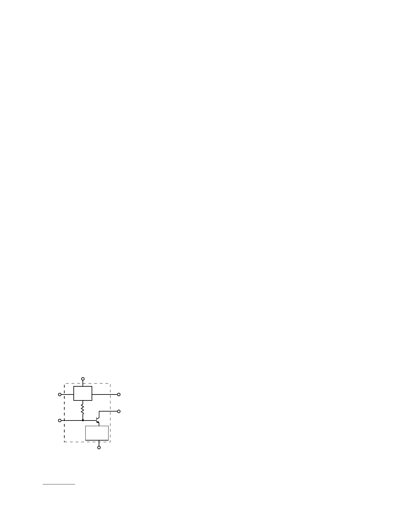
fied schematic diagram of the
INA-12063 is shown in Figure 9.
The result is a versatile gain stage
that can be operated from a single
+1.5 to +5 volt power supply with
the device current set by the user.
The INA-12063 is designed for use
in battery powered equipment
demanding high performance
with low supply voltages and
minimal current drain. Typical
applications for the INA-12063
include low noise RF amplifiers,
IF amplifiers, gain and buffer
stages through 2 GHz. The
INA-12063 is an excellent choice
for use in cellular and cordless
telephones, PCS, W/LAN’s, RF
modems and other commercial
wireless equipment.
GND 2
RF
INPUT
Vd
ACTIVE
BIAS
CIRCUIT
RF
TRANSISTOR
RF
FEEDBACK
NETWORK
GND 1
Ibias
RF
OUTPUT
and Vc
Figure 9. INA-12063 Schematic.
Description
The active bias circuit solves
three problems normally encoun-
tered with traditional approaches
for biasing discrete transistors.
First, as an active bias circuit, the
emitter of the RF transistor is DC
grounded. This permits the
collector current to be controlled
without the need for resistors
and/or bypass capacitors in the
emitter that may degrade RF
performance.
Second, the internal bias circuit
greatly simplifies the design tasks
commonly associated with bias-
ing transistors, such as accurately
regulating the collector current,
allowing for variations in hFE,
making a non-intrusive DC
connection to the base of the
transistor, and stabilizing current
over temperature.
And, third, the integrated bias
circuit eliminates the cost, parts
count, and associated PCB space
required for as many as 8 addi-
tional DC components.
The integrated bias control circuit
is very easy to use. For most
applications, the collector current
for the RF transistor can be set
with a single resistor.
The geometry of the integrated
RF transistor is designed to
provide an excellent balance
between low noise figure, high
gain, and good dynamic range
while retaining practical imped-
ance matching levels. The operat-
ing current is typically in the 1 to
10 mA range.
The integrated RF feedback
contains an inductive element in
the emitter circuit of the RF
transistor. This series feedback
configuration is of the type often
implemented in discrete transis-
tor designs for the purpose of
improving stability and bringing
the optimum noise match at the
input of the transistor closer to
50␣ Ω. The result is that for many
applications, a simple, series
inductor is often all that is needed
to adequately match the input of
the INA-12063 to 50 Ω.
In contrast to amplifiers that use
resistive feedback to achieve
broadband 50 Ω input and output
matches, the INA-12063 leaves
the designer with the flexibility of
optimizing performance for a
particular frequency band. For
example, frequency selective
input and output impedance
matching circuits can be used to
tune for optimum NF, maximum
output power, low input VSWR,
or to tailor the passband response
to eliminate undesirable gain
responses.
Setting the Bias Current
The integrated, active bias circuit
is a 10:1 current mirror. The
current mirror forces the collec-
tor current in the RF transistor to
be approximately 10 times the
current supplied to the Ibias pin.
In normal use, a voltage between
+1.5 and +5 volts, is applied to
both the Vd and Vc terminals of
the INA-12063. Although normally
connected to the same supply
voltage, it is not necessary that
both Vd and Vc be at the same
voltage.
The collector current of the RF
transistor is then set by injecting
a small control current into the
Ibias pin that is approximately
1/10 of the desired collector
current.
1 U.S. Patent Number 5436595
6-123
Share Link: 