232ACB Ver la hoja de datos (PDF) - Intersil
Número de pieza
componentes Descripción
Fabricante
232ACB Datasheet PDF : 10 Pages
| |||
HIN232A
Absolute Maximum Ratings
VCC to Ground. . . . . . . . . . . . . . . . . . . . . . (GND -0.3V) <VCC < 6V
V+ to Ground . . . . . . . . . . . . . . . . . . . . . . . . (VCC -0.3V) <V+ < 12V
V- to Ground. . . . . . . . . . . . . . . . . . . . . . . . -12V < V- < (GND +0.3V)
Input Voltages
TIN . . . . . . . . . . . . . . . . . . . . . . . . . . . . . -0.3V < VIN < (V+ +0.3V)
RIN . . . . . . . . . . . . . . . . . . . . . . . . . . . . . . . . . . . . . . . . . . . . . . . . . ±30V
Output Voltages
TOUT . . . . . . . . . . . . . . . . . . . .(V- -0.3V) < VTXOUT < (V+ +0.3V)
ROUT . . . . . . . . . . . . . . . . . (GND -0.3V) < VRXOUT < (V+ +0.3V)
Short Circuit Duration
TOUT . . . . . . . . . . . . . . . . . . . . . . . . . . . . . . . . . . . . . . Continuous
ROUT . . . . . . . . . . . . . . . . . . . . . . . . . . . . . . . . . . . . . . Continuous
ESD Classification . . . . . . . . . . . . . . . . . . . . See Specification Table
Thermal Information
Thermal Resistance (Typical, Note 1)
θJA (oC/W)
16 Ld SOIC (N) Package . . . . . . . . . . . . . . . . . . . . .
105
16 Ld SOIC (W) Package. . . . . . . . . . . . . . . . . . . . .
110
16 Ld PDIP Package*. . . . . . . . . . . . . . . . . . . . . . . .
85
Maximum Junction Temperature (Plastic Package) . . . . . .150oC
Maximum Storage Temperature Range . . . . . . . . . . -65oC to 150oC
Maximum Lead Temperature (Soldering 10s) . . . . . . . . . . . . .300oC
(SOIC - Lead Tips Only)
*Pb-free PDIPs can be used for through hole wave solder processing
only. They are not intended for use in Reflow solder processing
applications.
Operating Conditions
Temperature Range
HIN232ACX . . . . . . . . . . . . . . . . . . . . . . . . . . . . . . . . 0oC to 70oC
CAUTION: Stresses above those listed in “Absolute Maximum Ratings” may cause permanent damage to the device. This is a stress only rating and operation of the
device at these or any other conditions above those indicated in the operational sections of this specification is not implied.
NOTE:
1. θJA is measured with the component mounted on a low effective thermal conductivity test board in free air. See Tech Brief TB379 for details.
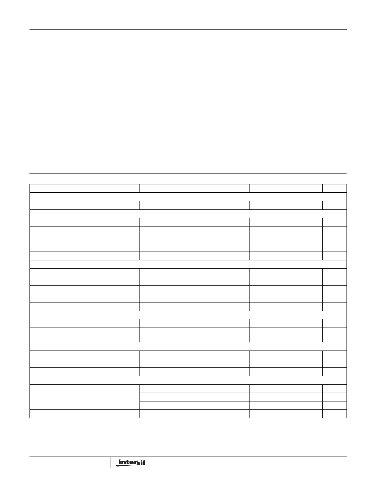
Electrical Specifications Test Conditions: VCC = +5V ±10%, C1-C4 = 0.1µF; TA = Operating Temperature Range
PARAMETER
TEST CONDITIONS
MIN
TYP
MAX UNITS
SUPPLY CURRENTS
Power Supply Current, ICC
No Load, TA = 25oC
LOGIC AND TRANSMITTER INPUTS, RECEIVER OUTPUTS
-
5
10
mA
Input Logic Low, VlL
Input Logic High, VlH
Transmitter Input Pullup Current, IP
TTL/CMOS Receiver Output Voltage Low, VOL
TTL/CMOS Receiver Output Voltage High, VOH
RECEIVER INPUTS
TIN
TIN
TIN = 0V
IOUT = 3.2mA
IOUT = -1mA
-
-
0.8
V
2.0
-
-
V
-
15
200
µA
-
0.1
0.4
V
3.5
4.6
-
V
RS-232 Input Voltage Range, VIN
Receiver Input Impedance, RIN
Receiver Input Low Threshold, VIN (H-L)
Receiver Input High Threshold, VIN (L-H)
Receiver Input Hysteresis, VHYST
TIMING CHARACTERISTICS
VIN = ±3V, TA = 25oC
VCC = 5V, TA = 25oC
VCC = 5V, TA = 25oC
VCC = 5V
-30
-
+30
V
3.0
5.0
7.0
kΩ
-
1.2
-
V
-
1.7
2.4
V
0.2
0.5
1.0
V
Transmitter, Receiver Propagation Delay, tPD
-
Transition Region Slew Rate, SRT
RL = 3kΩ, CL = 1000pF, Measured from +3V to
3
-3V or -3V to +3V, (Note 2) 1 Transmitter Switching
0.5
10
µs
20
45
V/µs
TRANSMITTER OUTPUTS
Output Voltage Swing, TOUT
Output Resistance, TOUT
RS-232 Output Short Circuit Current, ISC
ESD PERFORMANCE
Transmitter Outputs, 3kΩ to Ground
VCC = V+ = V- = 0V, VOUT = ±2V
TOUT Shorted to GND
±5
±9
±10
V
300
-
-
Ω
-
±10
-
mA
RS-232 Pins
(TOUT, RIN)
Human Body Model
IEC1000-4-2 Contact Discharge
-
±15
-
kV
-
±8
-
kV
IEC1000-4-2 Air Gap (Note 3)
-
±15
-
kV
All Other Pins
Human Body Model
-
±2
-
kV
NOTES:
2. Guaranteed by design.
3. Meets level 4.
3
Share Link: 