HFA3667 Ver la hoja de datos (PDF) - Intersil
Número de pieza
componentes Descripción
Fabricante
HFA3667 Datasheet PDF : 6 Pages
| |||
HFA3667
Absolute Maximum Ratings
Thermal Information
Supply Voltage . . . . . . . . . . . . . . . . . . . . . . . . . . . . . . . . -0.3 to 3.6V
Voltage on Any Other Pin . . . . . . . . . . . . . . . . . . . -0.3 to VCC +0.3V
Operating Conditions
Supply Voltage Range . . . . . . . . . . . . . . . . . . . . . . . . . .2.7V to 3.3V
Thermal Resistance (Typical, Note 1)
θJA (oC/W)
SSOP Package . . . . . . . . . . . . . . . . . . . . . . . . . . . .
88
Maximum Junction Temperature (Plastic Package) . . . . . . . . . 150oC
Maximum
Maximum
Maximum
Temperature Range . . . . . . . . . . . .
Storage Temperature Range . . . . .
Lead Temperature (Soldering 10s).
......-6.-45.o0.Co.C.≤.≤T. TA. A.≤≤13580050oooCCC
(Lead Tips Only)
CAUTION: Stresses above those listed in “Absolute Maximum Ratings” may cause permanent damage to the device. This is a stress only rating and operation
of the device at these or any other conditions above those indicated in the operational sections of this specification is not implied.
NOTE:
1. θJA is measured with the component mounted on an evaluation PC board in free air.
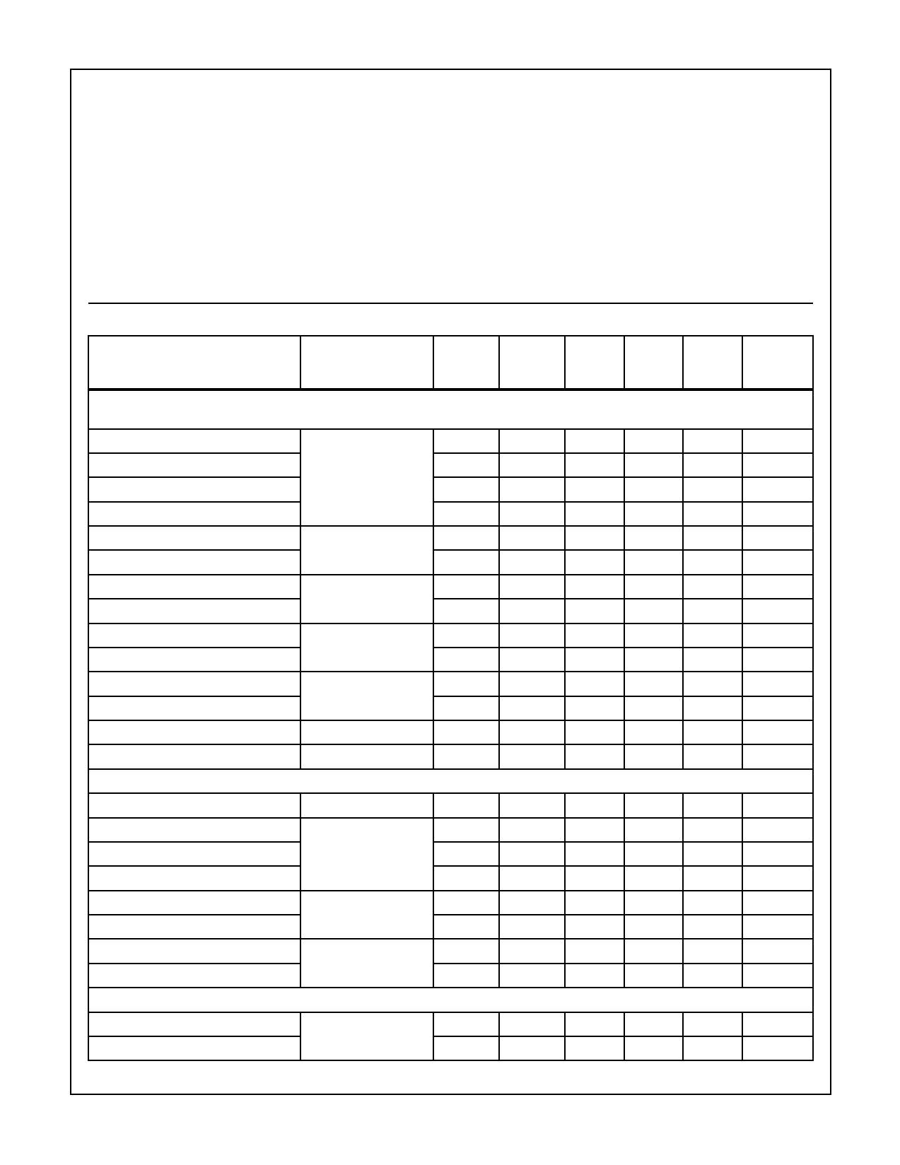
Electrical Specifications VCC = 2.7V, LO_IN = -3dBm, AGC_CTRL = 0.7VDC (Max Gain), TXM_IF = -30dBm
PARAMETER
(NOTE 2)
TEST
TEMP
TEST CONDITION
LEVEL
(oC)
MIN
TYP
MAX
UNITS
OVERALL CASCADED PERFORMANCE: LO_IN = -3dBm at 980MHz, TXM_IF = Differential -30dBm, at 130MHz, Interstage Filter
Insertion Loss of -3.7dB with an LO rejection of 35dB. Refer to applications diagram
Power Gain 250Ω In, 50Ω Out
Voltage Gain 250Ω In, 50Ω oUt
SSB NF
P1dBO
Refer to applications di-
A
agram and single to dif-
ferential input network.
B
(0dB Attenuation)
B
AGC_CTRL = 0.7V
A
25
25
31.9
35
25
18
23
28
25
-
15
-
25
11.4
13.8
-
dB
dB
dB
dBm
SSB NF
P1dBO
AGC_CTRL set for
10dB attenuation
B
25
-
15
-
dB
A
25
-
7.2
-
dBm
SSB NF
P1dBO
AGC_CTRL set for
20dB attenuation
B
25
-
15.5
-
dB
A
25
-
-7.4
-
dBm
SSB NF
P1dBO
AGC_CTRL set for
30dB attenuation
B
25
-
17.8
-
dB
A
25
-
-22
-
dBm
SSB NF
P1dBO
AGC_CTRL set for
40dB attenuation
B
25
-
24
-
dB
A
25
-
-35.9
-
dBm
Gain Flatness Across 825 to 850MHz (0dB Attenuation)
B
25
-1.7
-
+1.7
dB
LO Leakage
(0dB attenuation)
A
25
-
-43
-30
dB
CASCADED AMPLIFIERS SPECIFICATIONS AT 850MHz
RF Frequency Range (typical)
B
25
825
-
850
MHz
Power/Voltage Gain
SSB NF
(0dB Attenuation)
B
25
-
22
-
dB
AGC_CTRL = 0.7V
B
25
-
7.4
-
dB
P1dBO
B
25
-
14.5
-
dBm
SSB NF
P1dBO
AGC_CTRL set for
10dB attenuation
B
25
-
8.2
-
dB
B
25
-
9.5
-
dBm
SSB NF
P1dBO
AGC_CTRL set for
20dB attenuation
B
25
-
11.8
-
dB
B
25
-
-8.2
-
dBm
CASCADED AMPLIFIERS SPECIFICATIONS AT 850MHz
SSB NF
P1dBO
AGC_CTRL set for
30dB attenuation
B
25
-
17.9
-
dB
B
25
-
-22
-
dBm
3
Share Link: 