HFA3600 Ver la hoja de datos (PDF) - Intersil
Número de pieza
componentes Descripción
Fabricante
HFA3600 Datasheet PDF : 16 Pages
| |||
HFA3600
Absolute Maximum Ratings
Supply Voltage . . . . . . . . . . . . . . . . . . . . . . . . . . . . . . . -0.3 to +6.0V
Voltage on Any Other Pin. . . . . . . . . . . . . . . . . . . . -0.3 to VCC+0.3V
VCC to VCC Decouple . . . . . . . . . . . . . . . . . . . . . . . . . -0.3 to +0.3V
Any GND to GND. . . . . . . . . . . . . . . . . . . . . . . . . . . . . -0.3 to +0.3V
Operating Conditions
Temperature Range . . . . . . . . . . . . . . . . . . . . . . . -40oC ≤ TA ≤ 85oC
Supply Voltage Range . . . . . . . . . . . . . . . . . . . . . . . . . . . 4.0 to 5.5V
Thermal Information
Thermal Resistance (Typical, Note 1)
θJA (oC/W)
SOIC Package . . . . . . . . . . . . . . . . . . . . . . . . . . . . .
125
Maximum Package Power Dissipation at 25oC . . . . . . . . . . . . . . 1W
Maximum Junction Temperature (Plastic Package) . . . . . . . .150oC
Maximum
Maximum
Storage Temperature Range .
Lead Temperature (Soldering
....
10s)
.
.
.-65oC
......
≤ TA
....
≤ 150oC
. .300oC
(Lead Tips Only)
CAUTION: Stresses above those listed in “Absolute Maximum Ratings” may cause permanent damage to the device. This is a stress only rating and operation of the
device at these or any other conditions above those indicated in the operational sections of this specification is not implied.
NOTE:
1. θJA is measured with the component mounted on an evaluation PC board in free air.
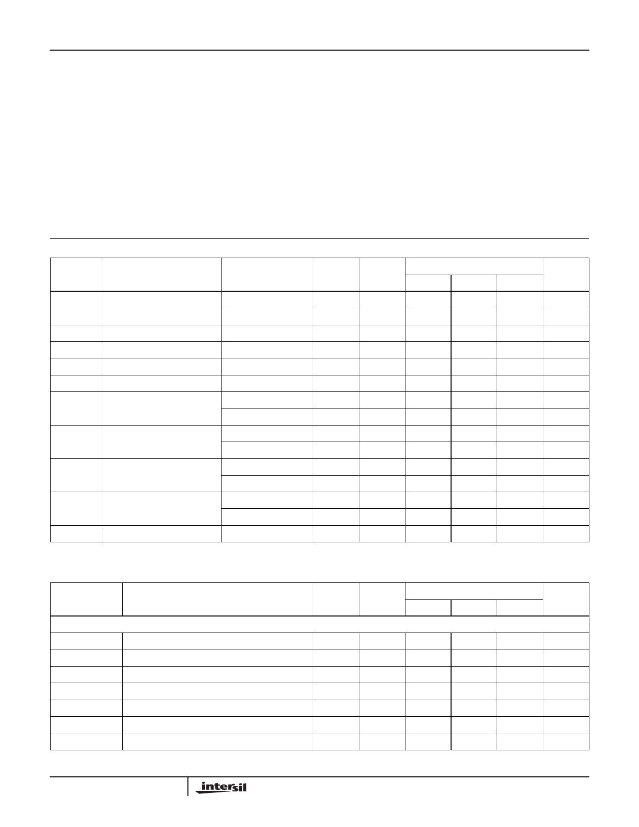
DC Electrical Specifications
SYMBOL
PARAMETER
ICC
Total Supply Current at 5V
VIH
VIL
IIL
IIH
VLNA-IN
Shutdown Logic High
Shutdown Logic Low
Shutdown Input Current
Shutdown Input Current
LNA Input DC Level
VLNA-OUT LNA Output DC Level
VMX-RF Mixer RFIN DC Level
VMX-LO Mixer LOIN DC Level
tOFF, ON Shutdown On-Off-On Time
CONDITION
Normal PD = 2V
Shutdown PD = 0.8V
Normal Mode
Shutdown Mode
PD = 0.4V
PD = 2.4V
Normal Mode
Shutdown Mode
Normal Mode
Shutdown Mode
Normal Mode
Shutdown Mode
Normal Mode
Shutdown Mode
TEST
LEVEL
A
A
A
A
A
A
A
A
A
A
A
A
A
A
B
TEMP
(oC)
25
25
25
25
25
25
25
25
25
25
25
25
25
25
25
ALL GRADES
MIN
TYP
MAX
-
11.3
12.5
-
250
375
2
-
VCC
-0.3
-
0.8
-200
-150
-100
-45
-24
-3
-
0.79
-
-
0.0
-
-
4.9
-
-
5.0
-
-
0.79
-
-
0.0
-
-
2.1
-
-
0.0
-
-
10
-
UNITS
mA
µA
V
V
µA
µA
V
V
V
V
V
V
V
V
µs
AC Electrical Specifications All Characterization Results have been Obtained with the Use of a
Standard Evaluation Board.
SYMBOL
PARAMETER
TEST
LEVEL
TEMP
(oC)
ALL GRADES
MIN
TYP
MAX
LNA (VCC = +5V, TA = 25oC, Test Figure 1 and f = 900MHz Unless Otherwise Noted In Characterization Curves)
S21LNA
LNA Gain
B
25
11.8
12.8
13.8
S12LNA
LNA Reverse Isolation
B
25
-
23
-
S11LNA
LNA Input Return Loss
B
25
6.0
7.3
-
S22LNA
LNA Output Return Loss
B
25
10.0
13.0
-
P-1dBLNA
LNA Output 1-dB Gain Compression Point
B
25
-
-2.0
-
IP3LNA
LNA Output 3rd-Order Intercept
B
25
+11.2
+12.8
-
NFLNA
LNA Noise Figure
B
25
-
2.30
2.60
UNITS
dB
dB
dB
dB
dBm
dBm
dB
2
Share Link: 