HDMP-1687 Ver la hoja de datos (PDF) - HP => Agilent Technologies
Número de pieza
componentes Descripción
Fabricante
HDMP-1687
HP => Agilent Technologies

HDMP-1687 Datasheet PDF : 16 Pages
| |||
Timing Characteristics for Gigabit Ethernet – Receiver Section
T = 0°C Ambient to +85°C Case, VCC = 3.15 V to 3.45 V
Symbol
Parameter
Units Min. Typ.
f_lock
Frequency Lock at Powerup
µs
b_sync[1,2] Bit Sync Time
bits
trxsetup
RX [0:3][0:9] Output Setup Time (Data Valid Before Clock)
ns
2.5
trxhold
RX [0:3][0:9] Output Hold Time (Data Valid After Clock)
ns
2.0
Tduty
tA-B
t_rxlat[3]
RC [0:3][0] and RC [0:3][1] Duty Cycle
%
40
Rising Edge Time Difference between RBC0 and RBC1 (Half Rate) ns
7.5
Receiver Latency
ns
20.7
bits
26.0
Max.
500
2500
60
8.5
Notes:
1. This is the recovery time for input phase jumps, per the Fibre Channel Specification X3.230-1994 FC-PH Standard, Sec 5.3.
2. Tested using CPLL = 0.1 µF.
3. The receiver latency, as shown in Figure 6, is defined as the time between receiving the first serial bit of a parallel data word (defined as the
edge of the first serial bit) and the clocking out of that parallel word (defined by the rising edge of the receive byte clock, RC[0:1]).
Timing Characteristics for Fibre Channel – Receiver Section
T = 0°C Ambient to +85°C Case, VCC = 3.15 V to 3.45 V
Symbol
Parameter
Units Min. Typ.
f_lock
Frequency Lock at Powerup
µs
b_sync[1,2] Bit Sync Time
bits
trxsetup
RX [0:3][0:9] Output Setup Time (Data Valid Before Clock)
ns
3.0
trxhold
Tduty
RX [0:3][0:9] Output Hold Time (Data Valid After Clock)
RC [0:3][0] and RC [0:3][1] Duty Cycle
ns
1.5
%
40
tA-B
t_rxlat[3]
Rising Edge Time Difference between RBC0 and RBC1 (Half Rate) ns
8.9
Receiver Latency
ns
22.4
bits
28.0
Max.
500
2500
60
9.9
Notes:
1. This is the recovery time for input phase jumps, per the Fibre Channel Specification X3.230-1994 FC-PH Standard, Sec 5.3.
2. Tested using CPLL = 0.1 µF.
3. The receiver latency, as shown in Figure 6, is defined as the time between receiving the first serial bit of a parallel data word (defined as the
edge of the first serial bit) and the clocking out of that parallel word (defined by the rising edge of the receive byte clock, RC[0:1]).
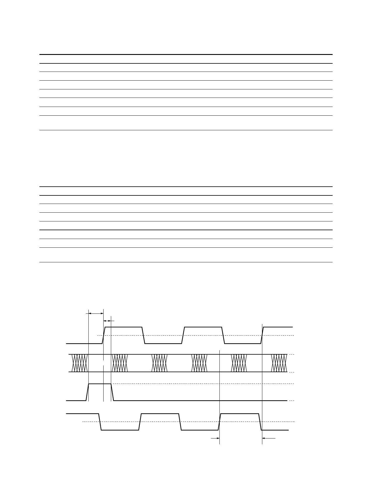
trxsetup
RC [0:3] [1]
trxhold
RX [0:3] [0:9]
K28.5+
DATA
SYNC
DATA
DATA
DATA
1.4 V
2.0 V
0.8 V
2.0 V
0.8 V
RC [0:3] [0]
Figure 5a. Receiver section timing (dual receive clocks).
5
1.4 V
tA-B
Share Link: