BSX20 Ver la hoja de datos (PDF) - Philips Electronics
Número de pieza
componentes Descripción
Fabricante
BSX20 Datasheet PDF : 8 Pages
| |||
Philips Semiconductors
NPN switching transistor
Product specification
BSX20
SYMBOL
PARAMETER
CONDITIONS
Switching times (between 10% and 90% levels)
ton
turn-on time
td
delay time
tr
rise time
toff
turn-off time
ts
storage time
tf
fall time
ton
turn-on time
td
delay time
tr
rise time
toff
turn-off time
ts
storage time
tf
fall time
ICon = 10 mA; IBon = 3 mA;
IBoff = −1.5 mA; see Fig.2, test
conditions A
ICon = 100 mA; IBon = 40 mA;
IBoff = −20 mA; see Fig.2, test
conditions B
MIN. TYP. MAX. UNIT
−
−
10 ns
−
−
4
ns
−
−
6
ns
−
−
30 ns
−
−
15 ns
−
−
15 ns
−
−
13 ns
−
−
3
ns
−
−
10 ns
−
−
35 ns
−
−
25 ns
−
−
10 ns
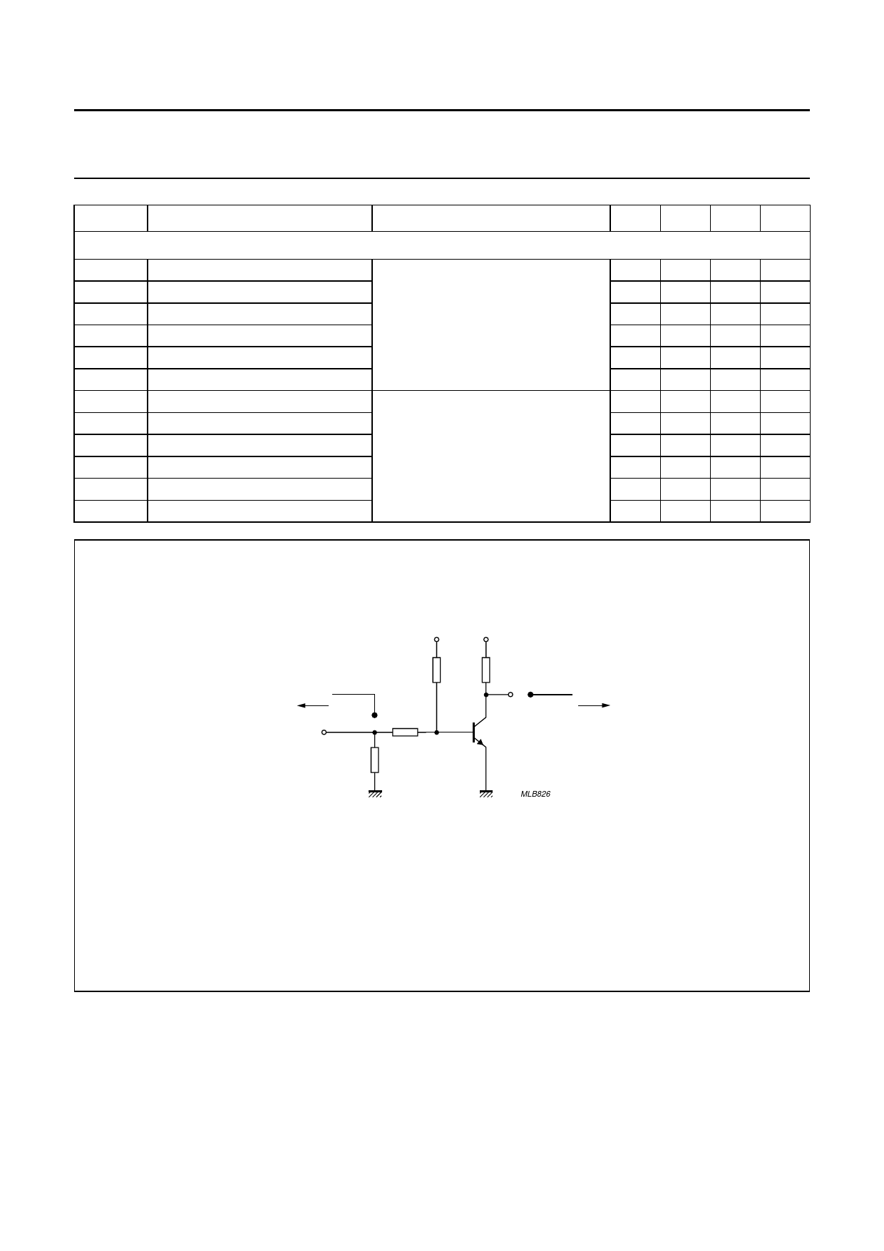
handbook, full pagewidth
VBB
VCC
(probe)
oscilloscope
450 Ω
Vi
RB
R2
R1
RC
Vo
(probe)
oscilloscope
450 Ω
DUT
MLB826
Test conditions A.
Vi = 0.5 to 4.2 V; T = 500 µs; tp = 10 µs; tr = tf ≤ 1 ns.
R1 = 56 Ω; R2 = 1 kΩ; RB = 1 kΩ; RC = 270 Ω.
VBB = 0.2 V; VCC = 2.7 V.
Test conditions B.
Vi = 0.5 to 4.52 V; T = 200 µs; tp = 10 µs; tr = tf ≤ 1 ns.
R1 = 100 Ω; R2 = 68 Ω; RB = 390 Ω; RC = 47 Ω.
VBB = −3 V; VCC = 4.6 V.
Fig.2 Test circuit for switching times.
1997 May 14
4
Share Link: 