LT1086 Ver la hoja de datos (PDF) - Linear Technology
Número de pieza
componentes Descripción
Fabricante
LT1086
Linear Technology

LT1086 Datasheet PDF : 16 Pages
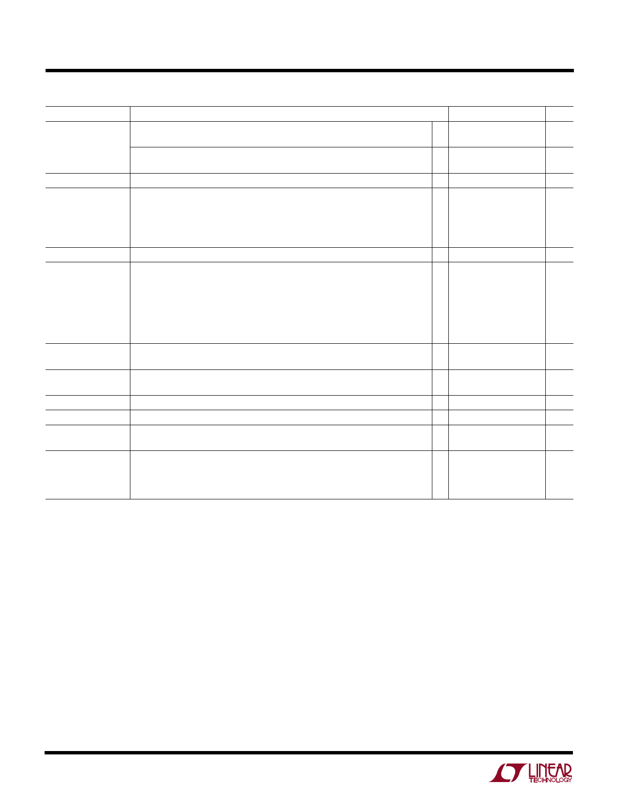
| |||
LT1086 Series
ELECTRICAL CHARACTERISTICS
PARAMETER
Current Limit
Minimum Load Current
Quiescient Current
Thermal Regulation
Ripple Rejection
Adjust Pin Current
CONDITIONS
LT1086/-2.85/-3.3/-3.6/-5/-12 (VIN – VOUT) = 5V
(VIN – VOUT) = 25V
LT1086H
(VIN – VOUT) = 5V
(VIN – VOUT) = 25V
LT1086/LT1086H (VIN – VOUT) = 25V (Note 4)
LT1086-2.85
LT1086-3.3
LT1086-3.6
LT1086-5
LT1086-12
VIN ≤ 18V
VIN ≤ 18V
VIN ≤ 18V
VIN ≤ 20V
VIN ≤ 25V
TA = 25°C, 30ms pulse
f = 120Hz, COUT = 25µF Tantalum, IOUT = 1.5A, (IOUT = 0.5A for LT1086H)
LT1086, LT1086H CADJ = 25µF, (VIN – VOUT) = 3V
LT1086-2.85
VIN = 6V
LT1086-3.3
VIN = 6.3V
LT1086-3.6
VIN = 6.6V
LT1086-5
VIN = 8V
LT1083-12
VIN = 15V
LT1086, LT1086H TJ = 25°C
Adjust Pin Current
Change
Temperature Stability
Long Term Stability
RMS Output Noise
(% of VOUT)
Thermal Resistance
Junction-to-Case
LT1086, LT1086H
10mA ≤ IOUT ≤ 1.5A, (0.5A for LT1086H)
1.5V ≤ (VIN – VOUT) ≤ 15V
TA = 125°C, 1000 Hrs.
TA = 25°C, 10Hz = ≤ f ≤ 10kHz
H Package: Control Circuitry/Power Transistor
K Package: Control Circuitry/Power Transistor
M Package: Control Circuitry/Power Transistor
T Package: Control Circuitry/Power Transistor
MIN TYP MAX UNITS
q 1.50 2.00
A
q 0.05 0.15
A
q 0.50 0.700
A
q 0.02 0.075
A
q
5
10
mA
q
5
10
mA
q
5
10
mA
q
5
10
mA
q
5
10
mA
q
5
10
mA
0.008 0.04 %/W
q 60 75
dB
q 60 72
dB
q 60 72
dB
q 60 72
dB
q 60 68
dB
q 54 60
dB
55
µA
q
120
µA
q
0.2 5
µA
q
0.5
%
0.3 1
%
0.003
%
15/20 °C/W
1.7/4.0 °C/W
1.5/4.0 °C/W
1.5/4.0 °C/W
The q denotes the specifications which apply over the full operating
temperature range.
Note 1: See thermal regulation specifications for changes in output voltage
due to heating effects. Line and load regulation are measured at a constant
junction temperature by low duty cycle pulse testing. Load regulation is
measured at the output lead ≈1/8" from the package.
Note 2: Line and load regulation are guaranteed up to the maximum power
dissipation of 15W (3W for the LT1086H). Power dissipation is determined
by the input/output differential and the output current. Guaranteed
maximum power dissipation will not be available over the full input/output
range. See Short-Circuit Current curve for available output current.
Note 3: Dropout voltage is specified over the full output current range of
the device. Test points and limits are shown on the Dropout Voltage curve.
Note 4: Minimum load current is defined as the minimum output current
required to maintain regulation. At 25V input/output differential the device
is guaranteed to regulate if the output current is greater than 10mA.
4
Share Link: