HA-2444883 Ver la hoja de datos (PDF) - Intersil
Número de pieza
componentes Descripción
Fabricante
HA-2444883 Datasheet PDF : 7 Pages
| |||
Specifications HA-2444/883
Absolute Maximum Ratings
Thermal Information
Voltage between V+ and V- Terminals . . . . . . . . . . . . . . . . . . . . 35V
Differential Input Voltage . . . . . . . . . . . . . . . . . . . . . . . . . . . . . . . 6V
Voltage at Either Input Terminal . . . . . . . . . . . . . . . . . . . . . . V+ to V-
Voltage on Digital Inputs. . . . . . . . . . . . . . GND +7.5V to GND -0.5V
Peak Output Current (≤10% Duty Cycle) . . . . . . . . . . . . . . . . . 40mA
Junction Temperature (TJ) . . . . . . . . . . . . . . . . . . . . . . . . . . +175oC
Storage Temperature Range . . . . . . . . . . . . . . . . . -65oC to +150oC
ESD Rating. . . . . . . . . . . . . . . . . . . . . . . . . . . . . . . . . . . . . . <2000V
Lead Temperature (Soldering 10s) . . . . . . . . . . . . . . . . . . . . +300oC
Thermal Resistance
θJA
θJC
CerDIP Package . . . . . . . . . . . . . . . . . . . 82oC/W 27oC/W
Package Power Dissipation Limit at +75oC for TJ ≤ +175oC
CerDIP Package . . . . . . . . . . . . . . . . . . . . . . . . . . . . . . . . . 1.22W
Package Power Dissipation Derating Factor Above +75oC
CerDIP Package . . . . . . . . . . . . . . . . . . . . . . . . . . . . . 12.2mW/oC
CAUTION: Stresses above those listed in “Absolute Maximum Ratings” may cause permanent damage to the device. This is a stress only rating and operation
of the device at these or any other conditions above those indicated in the operational sections of this specification is not implied.
Operating Conditions
Operating Temperature Range . . . . . . . . . . . . . . . . -55oC to +125oC
Operating Supply Voltage . . . . . . . . . . . . . . . . . . . . . . . . . ±12V to ±15V
VINCM ≤1/2(V+ - V-)
RL ≥1kΩ
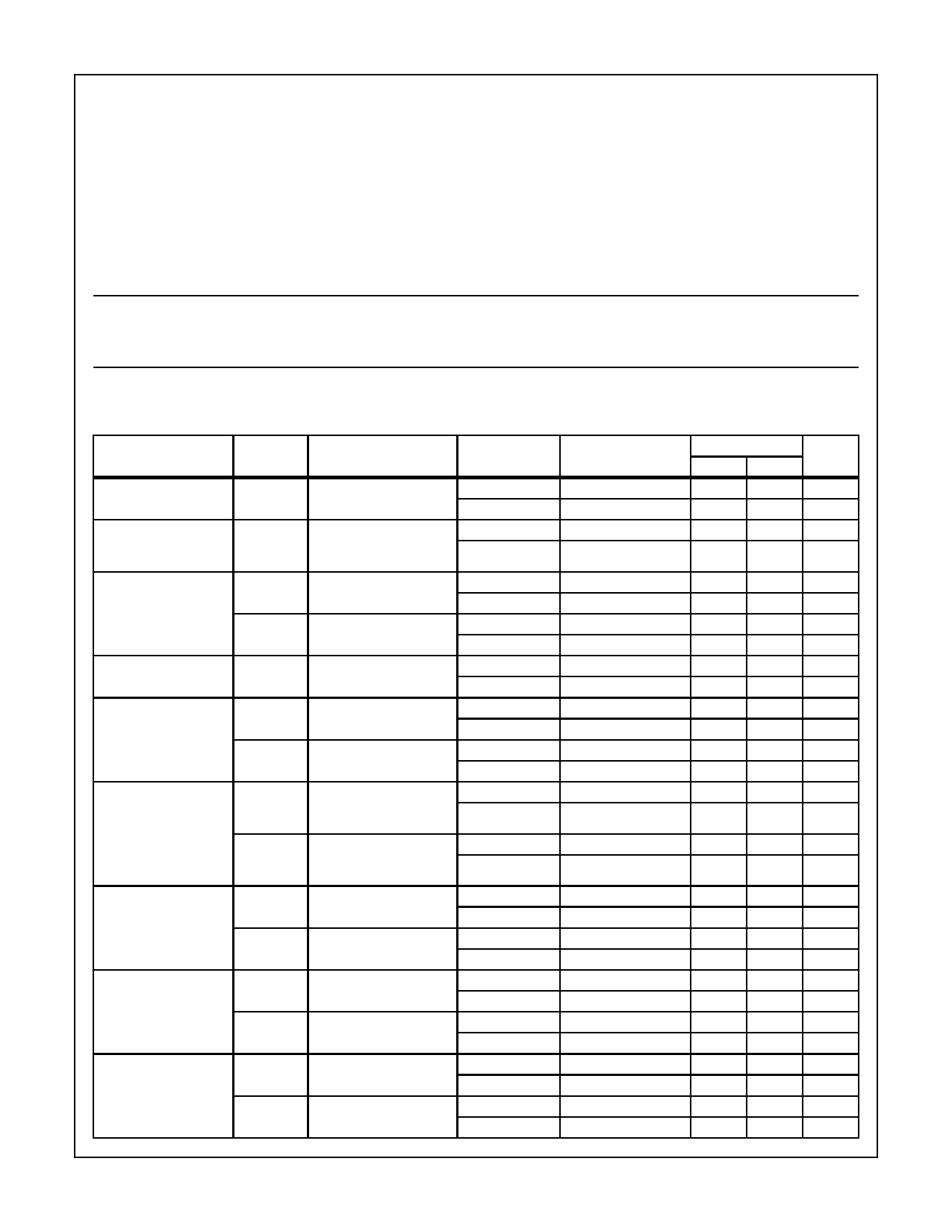
TABLE 1. DC ELECTRICAL PERFORMANCE CHARACTERISTICS
Device Tested at: VSUPPLY = ±15V, RSOURCE = 50Ω, RLOAD = 1kΩ, CLOAD ≤10pF, VOUT = 0V, VIL = 0.8V, VIH = 2.4V,
Unless Otherwise Specified.
PARAMETERS
Input Offset Voltage
SYMBOL
CONDITIONS
VIO
VCM = 0V
Channel to Channel
Offset Voltage
Mismatch
Input Bias Current
Input Offset Current
Large Signal Voltage
Gain
VIODEV VCM = 0V
+IB
-IB
IIO
+AVOL
VCM = 0V, +RS = 250Ω
-RS = 50Ω
VCM = 0V, +RS = 50Ω
-RS = 250Ω
VCM = 0V, +RS = 250Ω
-RS = 250Ω
VOUT = 0V and +5V
-AVOL VOUT = 0V and -5V
Common Mode
Rejection Ratio
Output Voltage Swing
+CMRR
-CMRR
+VOUT
∆VCM = +5V,
VOUT = -5V,
V+ = 10V, V- = -20V
∆VCM = -5V,
VOUT = +5V,
V+ = 20V, V- = -10V
-VOUT
Output Current
Output Current
(Device Disabled)
+IOUT
-IOUT
+DISAB
-DISAB
VOUT = -10V
RLOAD = OPEN
VOUT = 10V
RLOAD = OPEN
VOUT = 5V, VEN = 0.8V
RLOAD = OPEN
VOUT = -5V, VEN = 0.8V
RLOAD = OPEN
GROUP A
SUBGROUP
1
2, 3
1
2, 3
1
2, 3
1
2, 3
1
2, 3
4
5, 6
4
5, 6
1
2, 3
1
2, 3
1
2, 3
1
2, 3
1
2, 3
1
2, 3
1
2, 3
1
2, 3
TEMPERATURE
+25oC
+125oC, -55oC
+25oC
+125oC, -55oC
+25oC
+125oC, -55oC
+25oC
+125oC, -55oC
+25oC
+125oC, -55oC
+25oC
+125oC, -55oC
+25oC
+125oC, -55oC
+25oC
+125oC, -55oC
+25oC
+125oC, -55oC
+25oC
+125oC, -55oC
+25oC
+125oC, -55oC
+25oC
+125oC, -55oC
+25oC
+125oC, -55oC
+25oC
+125oC, -55oC
+25oC
+125oC, -55oC
LIMITS
MIN MAX
-7
7
-20
20
-
5
-
12
-15
15
-25
25
-15
15
-25
25
-4
4
-8
8
71
-
65
-
71
-
65
-
68
-
68
-
68
-
68
-
10
-
10
-
-
-10
-
-10
25
-
25
-
-
-25
-
-25
-
860
-
860
-
860
-
860
UNITS
mV
mV
mV
mV
µA
µA
µA
µA
µA
µA
dB
dB
dB
dB
dB
dB
dB
dB
V
V
V
V
mA
mA
mA
mA
µA
µA
µA
µA
Spec Number 511091-883
3-2
Share Link: 