LT1959 Ver la hoja de datos (PDF) - Linear Technology
Número de pieza
componentes Descripción
Fabricante
LT1959 Datasheet PDF : 24 Pages
| |||
LT1959
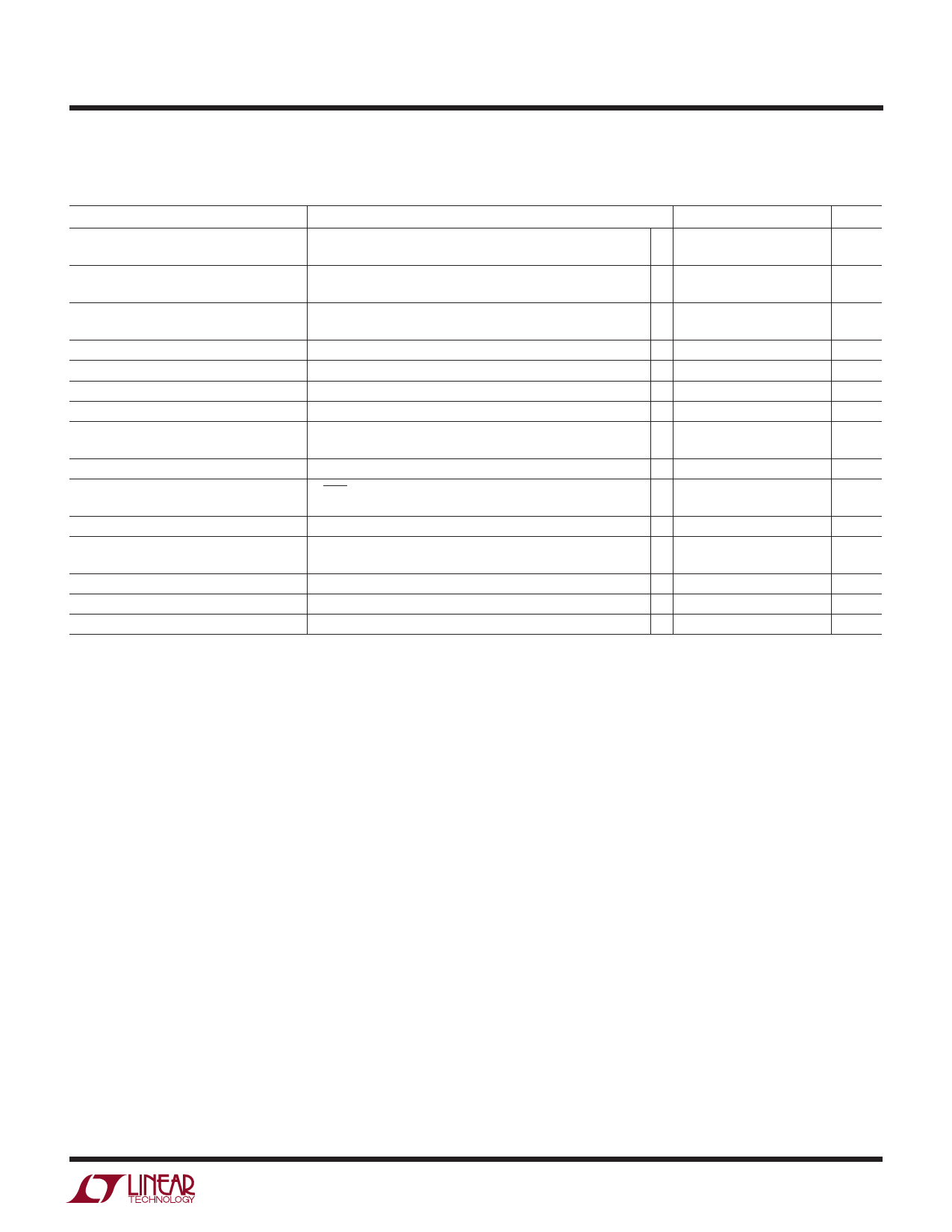
ELECTRICAL CHARACTERISTICS The q denotes the specifications which apply over the full operating
temperature range, otherwise specifications are at TA = 25°C, TJ = 25°C, VIN = 5V, VC = 1.5V, Boost = VIN + 5V, switch open, unless
otherwise noted.
PARAMETER
Switch On Resistance (Note 7)
Maximum Switch Duty Cycle
Switch Frequency
Switch Frequency Line Regulation
Frequency Shifting Threshold on FB Pin
Minimum Input Voltage (Note 3)
Minimum Boost Voltage (Note 4)
Boost Current (Note 5)
Input Supply Current (Note 6)
Shutdown Supply Current
Lockout Threshold
Shutdown Thresholds
Synchronization Threshold
Synchronizing Range
SYNC Pin Input Resistance
CONDITIONS
ISW = 4.5A
VFB = 1.05V
VC Set to Give 50% Duty Cycle
4.3V ≤ VIN ≤ 15V
∆f = 10kHz
ISW ≤ 4.5A
ISW = 1A
ISW = 4.5A
VSHDN = 0V, VSW = 0V, VC Open
VC Open
VC Open Device Shutting Down
Device Starting Up
MIN TYP MAX
0.07 0.1
q
0.13
90 93
q 86 93
460 500 540
q 440
560
q
0 0.15
q 0.5 0.7 1.0
q
4.0 4.3
q
2.3 3.0
q
20 35
q
90 140
q
3.8 5.4
15 50
q
75
q 2.3 2.38 2.46
q 0.13 0.37 0.60
q 0.25 0.45 0.7
q
1.5 2.2
580
1000
40
UNITS
Ω
Ω
%
%
kHz
kHz
%/ V
V
V
V
mA
mA
mA
µA
µA
V
V
V
V
kHz
kΩ
Note 1: Absolute Maximum Ratings are those values beyond which the life
of a device may be impaired.
Note 2: Gain is measured with a VC swing equal to 200mV above the
switching threshold level to 200mV below the upper clamp level.
Note 3: Minimum input voltage is not measured directly, but is guaranteed
by other tests. It is defined as the voltage where internal bias lines are still
regulated so that the reference voltage and oscillator frequency remain
constant. Actual minimum input voltage to maintain a regulated output will
depend on output voltage and load current. See Applications Information.
Note 4: This is the minimum voltage across the boost capacitor needed to
guarantee full saturation of the internal power switch.
Note 5: Boost current is the current flowing into the boost pin with the pin
held 5V above input voltage. It flows only during switch on time.
Note 6: Input supply current is the bias current drawn by the input pin
with switching disabled.
Note 7: Switch on resistance is calculated by dividing VIN to VSW voltage
by the forced current (4.5A). See Typical Performance Characteristics for
the graph of switch voltage at other currents.
3
Share Link: 