SAA1504T/N1 Ver la hoja de datos (PDF) - Philips Electronics
Número de pieza
componentes Descripción
Fabricante
SAA1504T/N1 Datasheet PDF : 16 Pages
| |||
Philips Semiconductors
Safety IC
Objective specification
SAA1504T
Disable mode
When the charge or discharge current exceeds the
specified maximum value, the disable mode is entered.
Detection of the maximum charge or discharge current is
only activated when the outputs are HIGH (CO = 1 and
DO = 1) as explained next.
If the safety IC is in the Power-down mode and a charge
current is detected (e.g. VVM = −0.6 V) the normal
operating mode will be entered when Vbat > 2.6 V.
Because of a minimum time in which the gate capacitors
have to be charged, VVM = −0.6 V for a small period, when
the safety IC is already in the normal operating mode.
VVM = −0.6 V could also occur when the battery is charged
with a current exceeding the maximum charge current.
To prevent that a maximum charge current is detected
when coming from the Power-down mode a delay is
included to ensure charging of both outputs CO and DO.
So entering of the disable mode is enabled when both
outputs CO and DO are fully charged or after a certain
delay. The delay is necessary to activate the current
protection even in case the outputs CO or DO can not be
fully charged.
The same applies for entering the disable mode when the
safety IC is in the discharge enable mode.
The delay of the current protection as a function of the
sense voltage VVM (for charge and discharge) is given in
Fig.5.
The disable mode is also entered when the junction
temperature exceeds 100 °C. When the temperature
drops below 60 °C and at the absence of a charger or load,
the safety IC will return to its previous mode.
Status output
The status of the safety IC is available on pin ST.
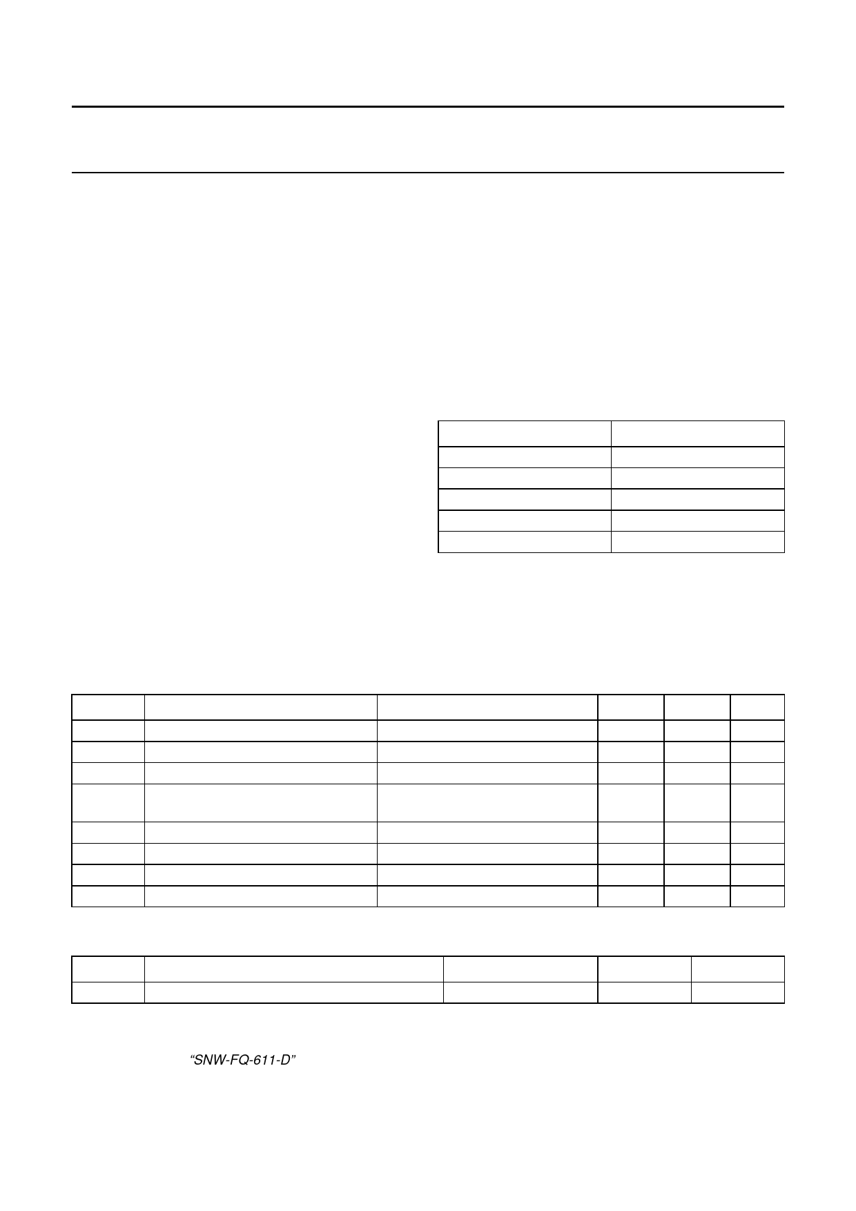
Table 1 Functional table of the status output
MODE
Normal operating
Charge inhibit
Discharge enable
Power-down
Disable
OUTPUT PIN ST
LOW
HIGH
LOW
LOW
HIGH (note 1)
Note
1. Only when a charger is connected.
LIMITING VALUES
In accordance with the Absolute Maximum Rating System (IEC 60134); voltages measured with respect to pin VSS.
SYMBOL
PARAMETER
CONDITION
MIN. MAX. UNIT
VCC
VCC(clamp)
ICC(clamp)
Vrev
positive battery sense input voltage
clamping voltage
clamping current
reverse charger voltage
VVM
VST
Tamb
Tstg
negative sense input voltage
voltage on pin ST
ambient temperature
storage temperature
DC constant
ICC(clamp) = 7 mA; t < 60 ms
Vrev = −(VCC − VVM);
VVM positive with respect to VCC
−0.3
+4.5
V
−
8.5
V
−
7
mA
−
20
V
VCC − 20 VCC + 20 V
VVM
VCC
V
−25
+80
°C
−55
+150
°C
THERMAL CHARACTERISTICS
SYMBOL
PARAMETER
Rth(j-a)
thermal resistance from junction to ambient
CONDITIONS
in free air
QUALITY SPECIFICATION
In accordance with “SNW-FQ-611-D” and JEDEC class III.
VALUE
160
UNIT
K/W
2000 Mar 07
7
Share Link: 