HPMX-5001-TY1 Ver la hoja de datos (PDF) - HP => Agilent Technologies
Número de pieza
componentes Descripción
Fabricante
HPMX-5001-TY1 Datasheet PDF : 15 Pages
| |||
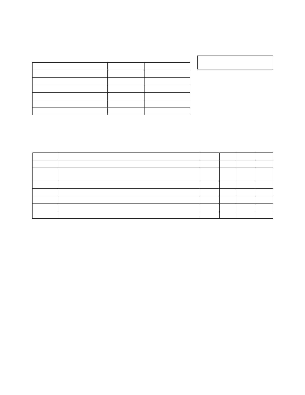
HPMX-5001 Absolute Maximum Ratings[1]
Parameter
Min.
Max.
VCC Supply Voltage
Voltage at Any Pin[4]
Power Dissipation[2,3]
-0.2 V
-0.2 V
8V
VCC + 0.2 V
600 mW
RF Input Power
Junction Temperature
Storage Temperature
-55°C
15 dBm
+150°C
+125°C
Thermal Resistance[2]:
θjc = 100°C/W
Notes:
1. Operation of this device in excess of
any of these parameters may cause
permanent damage.
2. TCASE = 25°C.
3. Derate at 10 mW/°C for TCASE > 90°C.
4. Except CMOS logic inputs – see
Summary Characterization Information
table.
HPMX-5001 Guaranteed Electrical Specifications
Unless otherwise noted, all parameters are guaranteed under the following conditions: VCC = 3.0 V. Test
results are based upon use of networks shown in test board schematic diagram (see Figure 28). Typical
values are for VCC = 3.0 V, TA = 25°C.
Symbol
Parameters and Test Conditions
Units Min. Typ. Max.
GC
Receive Conversion Gain[1]
Pout Transmitter Power Output
dB
12 14
Input[2]
2:1 output VSWR dBm
0
2
ICC Device Supply Current
Transmit Mode mA
Receive Mode mA
64 80
43 54
Synth Mode mA
15 19
Standby Mode (with DIVMC Set High) µA
1
50
VDIV DIV Single-Ended Swing[3]
VPP
0.7
1
Notes:
1. 50 Ω RF source, 100 MHz < IF < 300 MHz, 1.89 GHz RF. There is a 750 Ω resistor on chip between RXIF and RXIFB (pins 3 and 4). A
matching network from 750 Ω to 50 Ω is used for this measurement. Insertion loss of the matching network is included in the net
conversion gain figure. See Figure 28.
2. Signal injected into P3 in Figure 28 is -12.5 dBm.
3. DIV output AC coupled into a 2 kΩ || 10 pF load. See test board schematic diagram, Figure 28.
7-91
Share Link: 