AB28F400BX-T90 Ver la hoja de datos (PDF) - Intel
Número de pieza
componentes Descripción
Fabricante
AB28F400BX-T90 Datasheet PDF : 34 Pages
| |||
A28F400BX-T B
2 1 A28F400BX Memory Organization
2 1 1 BLOCKING
The A28F400BX uses a blocked array architecture
to provide independent erasure of memory blocks A
block is erased independently of other blocks in the
array when an address is given within the block ad-
dress range and the Erase Setup and Erase Confirm
commands are written to the CUI The A28F400BX
is a random read write memory only erasure is per-
formed by block
2 1 1 1 Boot Block Operation and Data
Protection
The 16-Kbyte boot block provides a lock feature for
secure code storage The intent of the boot block is
to provide a secure storage area for the kernel code
that is required to boot a system in the event of pow-
er failure or other disruption during code update
This lock feature ensures absolute data integrity by
preventing the boot block from being written or
erased when RP is not at 12V The boot block can
be erased and written when RP is held at 12V for
the duration of the erase or program operation This
allows customers to change the boot code when
necessary while providing security when needed
See the Block Memory Map section for address lo-
cations of the boot block for the A28F400BX-T and
A28F400BX-B
2 1 1 2 Parameter Block Operation
The A28F400BX has 2 parameter blocks (8 Kbytes
each) The parameter blocks are intended to provide
storage for frequently updated system parameters
and configuration or diagnostic information The pa-
rameter blocks can also be used to store additional
boot or main code The parameter blocks however
do not have the hardware write protection feature
that the boot block has The parameter blocks pro-
vide for more efficient memory utilization when deal-
ing with parameter changes versus regularly blocked
devices See the Block Memory Map section for ad-
dress locations of the parameter blocks for the
A28F400BX-T and A28F400BX-B
2 1 1 3 Main Block Operation
Four main blocks of memory exist on the
A28F400BX (3 x 128 Kbyte blocks and 1 x 96-Kbyte
blocks) See the following section on Block Memory
Map for the address location of these blocks for the
A28F400BX-T and A28F400BX-B products
2 1 2 BLOCK MEMORY MAP
Two versions of the A28F400BX product exist to
support two different memory maps of the array
blocks in order to accommodate different microproc-
essor protocols for boot code location The
A28F400BX-T memory map is inverted from the
A28F400BX-B memory map
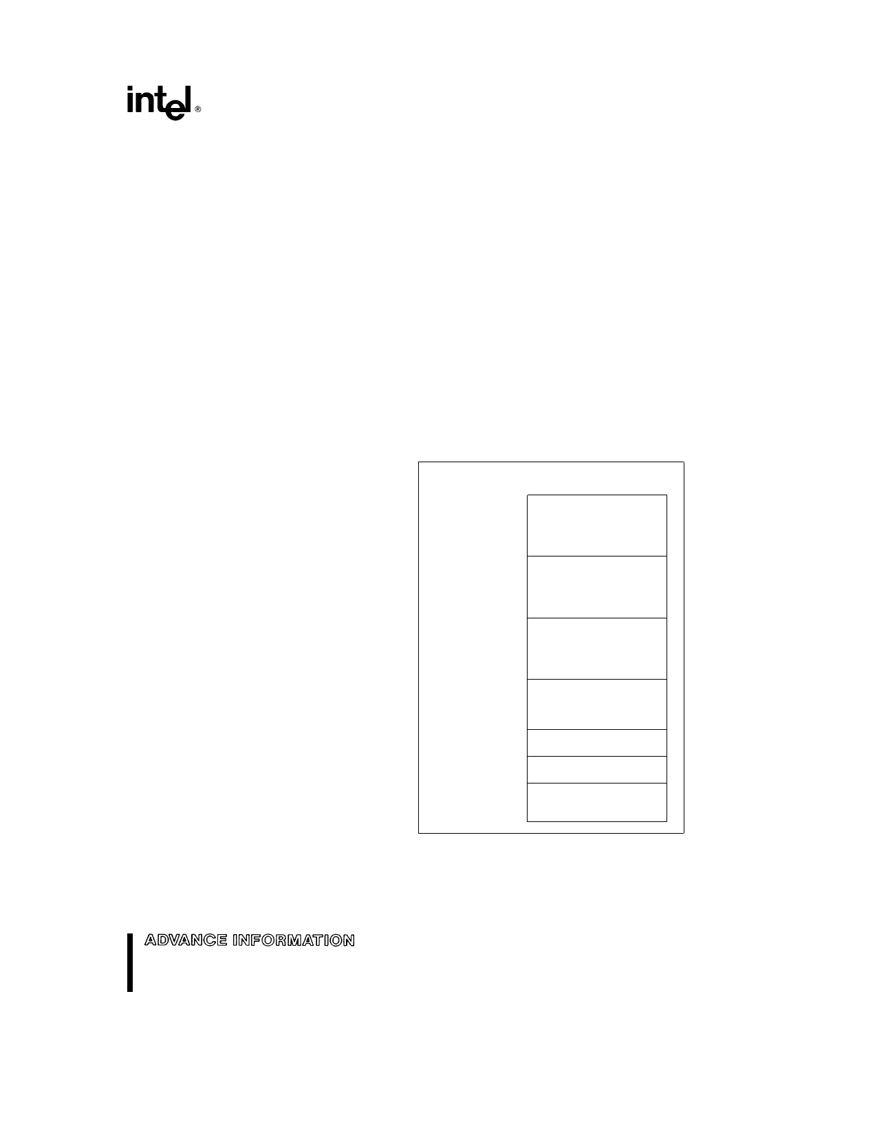
2 1 2 1 A28F400BX-B Memory Map
The A28F400BX-B device has the 16-Kbyte boot
block located from 00000H to 01FFFH to accommo-
date those microprocessors that boot from the bot-
tom of the address map at 00000H In the
A28F400BX-B the first 8-Kbyte parameter block re-
sides in memory space from 02000H to 02FFFH
The second 8-Kbyte parameter block resides in
memory space from 03000H to 03FFFH The 96-
Kbyte main block resides in memory space from
04000H to 0FFFFH The three 128-Kbyte main
block resides in memory space from 10000H to
1FFFFH 20000H to 2FFFFH and 30000H to
3FFFFH (word locations) See Figure 4
(Word Addresses)
3FFFFH
128-Kbyte MAIN BLOCK
30000H
2FFFFH
128-Kbyte MAIN BLOCK
20000H
1FFFFH
128-Kbyte MAIN BLOCK
10000H
0FFFFH
04000H
03FFFH
03000H
02FFFH
02000H
01FFFH
00000H
96-Kbyte MAIN BLOCK
8-Kbyte PARAMETER BLOCK
8-Kbyte PARAMETER BLOCK
16-Kbyte BOOT BLOCK
Figure 4 A28F400BX-B Memory Map
9
Share Link: 