7217(1997) Ver la hoja de datos (PDF) - Intersil
Número de pieza
componentes Descripción
Fabricante
7217 Datasheet PDF : 19 Pages
| |||
ICM7217
TABLE 1. ICM7217 MULTIPLEXED RATE CONTROL
SCAN
CAPACITOR
None
20pF
90pF
NOMINAL
OSCILLATOR
FREQUENCY
2.5kHz
1.25kHz
600Hz
DIGIT
REPETITION
RATE
625Hz
300Hz
150Hz
SCAN
CYCLE
TIME
(4 DIGITS)
1.6ms
3.2ms
8ms
The internal oscillator output has a duty cycle of
approximately 25:1, providing a short pulse occurring at the
oscillator frequency. This pulse clocks the four-state counter
which provides the four multiplex phases. The short pulse
width is used to delay the digit driver outputs, thereby provid-
ing inter-digit blanking which prevents ghosting. The digits
are scanned from MSD (D4) to LSD (D1). See Figure 1 for
the display digit multiplex timing.
During load counter and load register operations, the
multiplex oscillator is disconnected from the SCAN input and
is allowed to free-run. In all other conditions, the oscillator
may be directly overdriven to about 20kHz, however the
external oscillator signal should have the same duty cycle as
the internal signal, since the digits are blanked during the
time the external signal is at a positive level (see Figure 1).
To insure proper leading zero blanking, the interdigit blank-
ing time should not be less than about 2µs. Overdriving the
oscillator at less than 200Hz may cause display flickering.
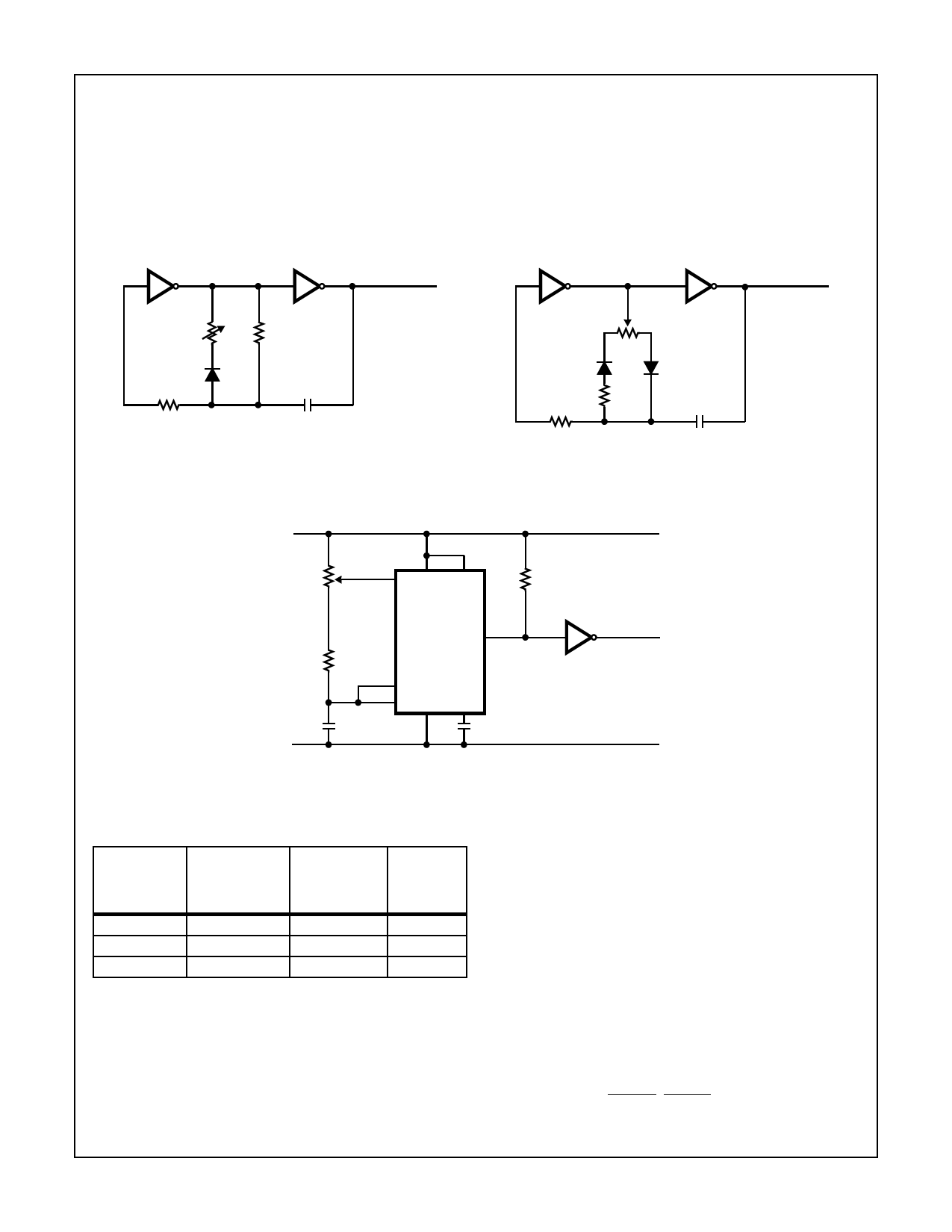
The display brightness may be altered by varying the duty
cycle. Figure 10 shows several variable-duty-cycle oscilla-
tors suitable for brightness control at the ICM7217 SCAN
input. The inverters should be CMOS CD4000 series and
the diodes may be any inexpensive device such as lN914.
Counting Control, STORE, RESET
As shown in Figure 2, the counter is incremented by the
rising edge of the COUNT INPUT signal when UP/DOWN is
high. It is decremented when UP/DOWN is low. A Schmitt
trigger on the COUNT INPUT provides hysteresis to prevent
double triggering on slow rising edges and permits operation
in noisy environments. The COUNT INPUT is inhibited dur-
ing reset and load counter operations.
The STORE pin controls the internal latches and
consequently the signals appearing at the 7-Segment and
BCD outputs. Bringing the STORE pin low transfers the con-
tents of the counter into the latches.
The counter is asynchronously reset to 0000 by bringing the
RESET pin low. The circuit performs the reset operation by
forcing the BCD input lines to zero, and “presetting” all four
decades of counter in parallel. This affects register loading; if
LOAD REGISTER is activated when the RESET input is low,
the register will also be set to zero. The STORE, RESET and
UP/DOWN pins are provided with pullup resistors of approxi-
mately 75kΩ.
BCD I/O Pins
The BCD I/O port provides a means of transferring data to
and from the device. The ICM7217 versions can multiplex
data into the counter or register via thumbwheel switches,
depending on inputs to the LOAD COUNTER or LOAD
REGISTER pins; (see below). When functioning as outputs,
the BCD I/O pins will drive one standard TTL load. Common
anode versions have internal pull down resistors and com-
mon cathode versions have internal pull up resistors on the
four BCD I/O lines when used as inputs.
LOADing the COUNTER and REGISTER
The BCD I/O pins, the LOAD COUNTER (LC), and LOAD
REGISTER (LR) pins combine to provide presetting and
compare functions. LC and LR are 3-level inputs, being self-
biased at approximately 1/2VDD for normal operation. With
both LC and LR open, the BCD I/O pins provide a multi-
plexed BCD output of the latch contents, scanned from MSD
to LSD by the display multiplex.
When either the LOAD COUNTER (Pin 12) or LOAD
REGISTER (Pin 11) is taken low, the drivers are turned off
and the BCD pins become high-impedance inputs. When LC
is connected to VDD, the count input is inhibited and the lev-
els at the BCD pins are multiplexed into the counter. When
LR is connected to VDD, the levels at the BCD pins are mul-
tiplexed into the register without disturbing the counter.
When both are connected to VDD, the count is inhibited and
both register and counter will be loaded.
The LOAD COUNTER and LOAD REGISTER inputs are
edge-triggered, and pulsing them high for 500ns at room
temperature will initiate a full sequence of data entry cycle
operations (see Figure 3). When the circuit recognizes that
either or both of the LC or LR pins input is high, the multiplex
oscillator and counter are reset (to D4). The internal
oscillator is then disconnected from the SCAN pin and the
preset circuitry is enabled. The oscillator starts and runs with
a frequency determined by its internal capacitor, (which may
vary from chip to chip). When the chip finishes a full 4-digit
multiplex cycle (loading each digit from D4 to D3 to D2 to D1
in turn), it again samples the LOAD REGISTER and LOAD
COUNTER inputs. If either or both is still high, it repeats the
load cycle, if both are floating or low, the oscillator is
reconnected to the SCAN pin and the chip returns to normal
operation. Total load time is digit “on” time multiplied by 4. lf
the Digit outputs are used to strobe the BCD data into the
BCD I/O inputs, the input must be synchronized to the
appropriate digit (Figure 3). Input data must be valid at the
trailing edge of the digit output.
When LR is connected to GROUND, the oscillator is
inhibited, the BCD I/O pins go to the high impedance state,
and the segment and digit drivers are turned off. This allows
the display to be used for other purposes and minimizes
power consumption. In this display off condition, the circuit
will continue to count, and the CARRY/BORROW, EQUAL,
ZERO, UP/DOWN, RESET and STORE functions operate
as normal. When LC is connected to ground, the BCD I/O
pins are forced to the high impedance state without disturb-
ing the counter or register. See “Control Input Definitions”
(Table 2) for a list of the pins that function as three-state self-
biased inputs and their respective operations.
Note that the ICM7217 and ICM7217B have been designed
to drive common anode displays. The BCD inputs are high
true, as are the BCD outputs.
9-19
Share Link: 