DLR2416 Ver la hoja de datos (PDF) - Infineon Technologies
NГәmero de pieza
componentes DescripciГіn
Fabricante
DLR2416
Infineon Technologies

DLR2416 Datasheet PDF : 7 Pages
| |||
Maximum Ratings
DC Supply Voltage ........................................вҖ“0.5 V to +7.0 Vdc
Input Voltage, Respect to GND
(all inputs) .......................................... вҖ“0.5 V to VCC +0.5 Vdc
Operating Temperature ..................................... вҖ“40В°C to +85В°C
Storage Temperature ....................................... вҖ“40В°C to +100В°C
Relative Humidity at 85В°C.................................................... 85%
Maximum Solder Temperature, 0.063" (1.59 mm)
below Seating Plane, t<5 sec ...................................... 260 В°C
Optical Characteristics
Spectral Peak Wavelength
Red ...................................................................... 660 nm typ.
HER ..................................................................... 630 nm typ.
Green .................................................................. 565 nm typ.
Character Height ............................................. 0.200" (5.08 mm)
Time Averaged Luminous Intensity(1) at VCC=5 V
Red................................................................ 60 Вөcd/LED typ.
HER ............................................................. 100 Вөcd/LED typ.
Green .......................................................... 120 Вөcd/LED typ.
LED to LED Intensity Matching at VCC=5 V .............1.8:1.0 max.
LED to LED Hue Matching (Green only)
at VCC=5 V ........................................................... Вұ 2 nm max.
Viewing Angle (off normal axis)
Horizontal ...............................................................Вұ 50В° max.
Vertical . .................................................................Вұ 75В° max.
Note 1: Peak luminous intensity values can be calculated by multiply-
ing these values by 7.
Figure 1. Top View
18 17 16 15 14 13 12 11 10
Pins and Functions
Pin Function
Pin
1
CE1 Chip Enable 10
2
CE2 Chip Enable 11
3
CLR Clear
12
4
CUE Cursor En-
able
13
5
CU Cursor Select 14
6
WR Write
15
7
A1 Digit Select
16
8
A0 Digit Select
17
9
VCC
18
Function
GND
D0 Data Input
D1 Data Input
D2 Data Input
D3 Data Input
D6 Data Input
D5 Data Input
D4 Data Input
BL Display Blank
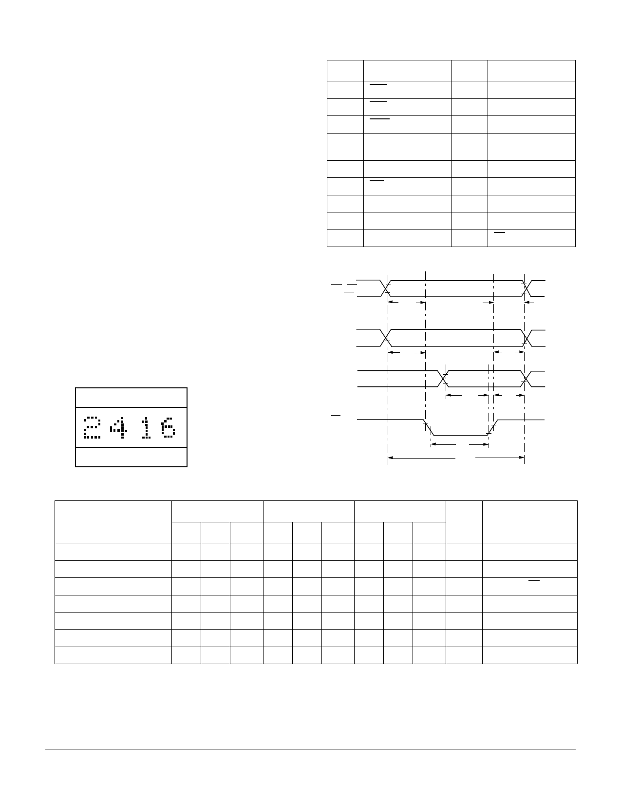
Figure 2. Timing characteristics вҖ”Write Cycle waveforms
CE1, CE2
CU, CLR
A0, A1
TCES
TCUS
TCLRD
TAS
TCEH
TCUH
TAH
2.0 V
0.8 V
2.0 V
0.8 V
D0-D6
TDS
TDH
2.0 V
0.8 V
digit 3 digit 2 digit 1 digit 0
1 2 3 456789
WR
2.0 V
0.8 V
TW
TACC
Note: These waveforms are not edge triggered.
DC Characteristics
Parameter
вҖ“40В°C
Min. Typ. Max.
+25В°C
Min. Typ. Max.
+85В°C
Units
Min. Typ. Max.
Condition
ICC 80 dots on
135 160
110 130
95 115 mA
ICC Cursor all dots at 50%
135
100
100 mA
ICC Blank
2.8 4.0
2.3 3.0
2.0 2.5 mA
IIL (all inputs)
30 60 120 25 50 100 20 40 80 ВөA
VIH (all inputs)
2.0
2.0
2.0
V
VIL (all inputs)
0.8
0.8
0.8 V
VCC
4.5 5.0 5.5 4.5 5.0 5.5 4.5 5.0 5.5 V
VCC=5 V
VCC=5 V
VCC=5 V, BL=0.8 V
VIN=0.8 V, VCC=5 V
VCC=5 V Вұ 0.5 V
VCC=5 V Вұ 0.5 V
DLR/DLO/DLG2416
5вҖ“2
Share Link: