PEB2466HV2.2(2001) Ver la hoja de datos (PDF) - Infineon Technologies
NГәmero de pieza
componentes DescripciГіn
Fabricante
PEB2466HV2.2
(Rev.:2001)
(Rev.:2001)
Infineon Technologies

PEB2466HV2.2 Datasheet PDF : 73 Pages
| |||
PEB 2466
PEF 2466
List of Tables
Page
Table 1
Table 2
Table 3
Table 4
Table 5
Table 6
Table 7
Table 8
Table 9
Table 10
Table 11
Table 12
Table 13
Table 14
Table 15
Table 16
Table 17
Table 18
Table 19
Table 20
Table 21
Table 22
Table 23
Table 24
Table 25
Table 26
Table 27
Table 28
Table 29
Table 30
Table 31
Table 32
Table 33
Table 34
Table 35
Table 36
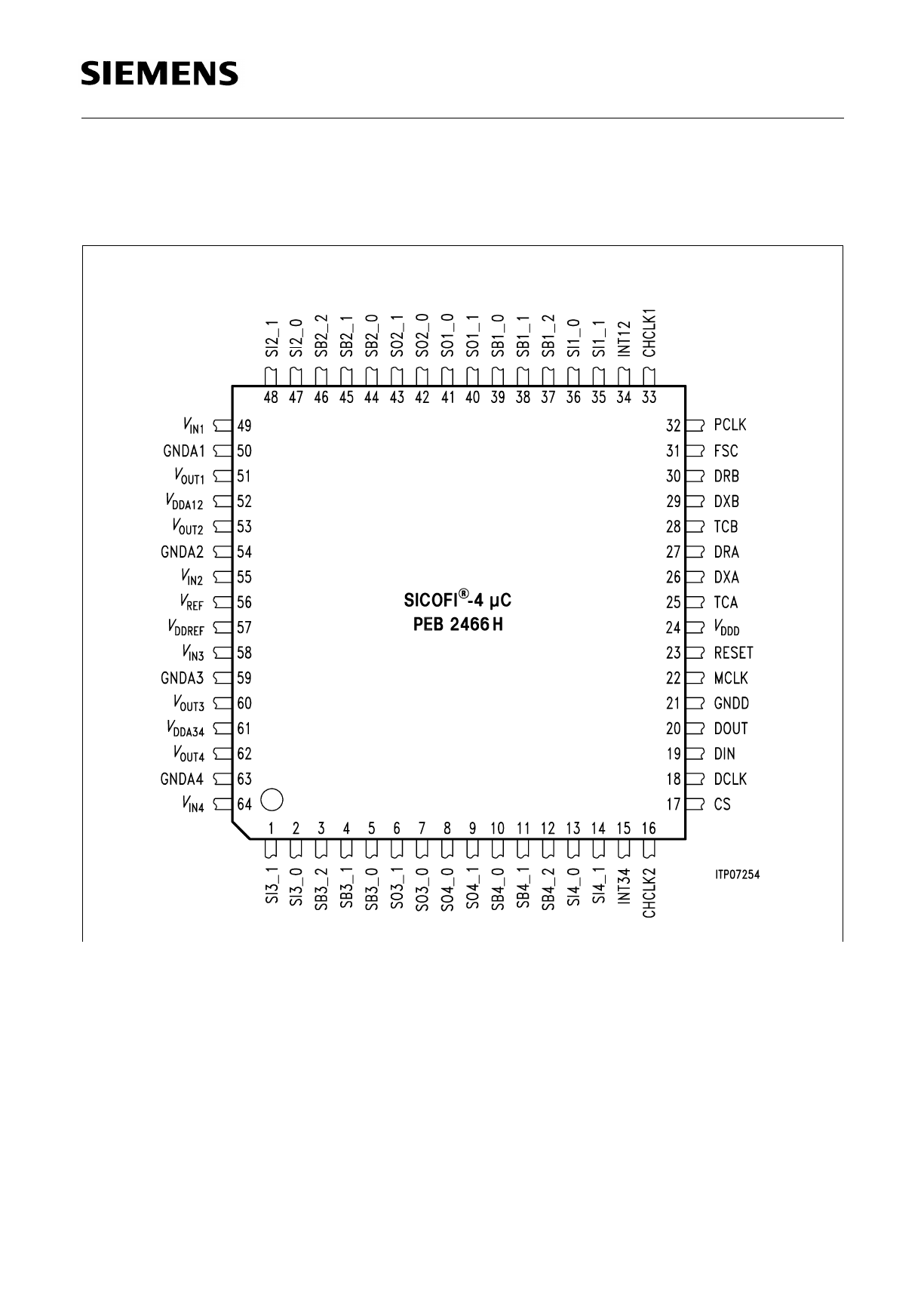
Pin Definitions and Functions . . . . . . . . . . . . . . . . . . . . . . . . . . . . . . . . 6
Register Values and Accessibility . . . . . . . . . . . . . . . . . . . . . . . . . . . . 13
Input and Output Pin Behavior. . . . . . . . . . . . . . . . . . . . . . . . . . . . . . . 13
Power Dissipation . . . . . . . . . . . . . . . . . . . . . . . . . . . . . . . . . . . . . . . . 14
Maximum Signal Levels . . . . . . . . . . . . . . . . . . . . . . . . . . . . . . . . . . . . 14
Analog Voltage Levels Corresponding to 0 dBm0-Level . . . . . . . . . . . 14
Gain Accuracy . . . . . . . . . . . . . . . . . . . . . . . . . . . . . . . . . . . . . . . . . . . 17
Gain Deviations with Input Level . . . . . . . . . . . . . . . . . . . . . . . . . . . . . 17
Attenuation with Frequency in Transmit and Receive Direction. . . . . . 18
Group Delay, Absolute Values . . . . . . . . . . . . . . . . . . . . . . . . . . . . . . . 18
Group Delay Distortion with Frequency . . . . . . . . . . . . . . . . . . . . . . . . 19
Idle Channel Noise in Transmit Direction. . . . . . . . . . . . . . . . . . . . . . . 19
Idle Channel Noise in Receive Direction . . . . . . . . . . . . . . . . . . . . . . . 19
Harmonic and Intermodulation Distortion. . . . . . . . . . . . . . . . . . . . . . . 20
Signal-to-Total Distortion Ratio Measured with Sine Wave . . . . . . . . . 20
Signal-to-Total Distortion Ratio Measured with Noise . . . . . . . . . . . . . 21
Crosstalk Between Channels . . . . . . . . . . . . . . . . . . . . . . . . . . . . . . . . 22
Out-of-Band Signals Applied to the Analog Inputs (VINx) . . . . . . . . . . 23
Out-of-Band Signals at the Analog Outputs (VOUTx) . . . . . . . . . . . . . 24
Transhybrid Loss . . . . . . . . . . . . . . . . . . . . . . . . . . . . . . . . . . . . . . . . . 26
Analog Interface Pins. . . . . . . . . . . . . . . . . . . . . . . . . . . . . . . . . . . . . . 29
PCM Interface Pins . . . . . . . . . . . . . . . . . . . . . . . . . . . . . . . . . . . . . . . 30
PCM Register Configuration Example . . . . . . . . . . . . . . . . . . . . . . . . . 31
Signaling Interface: Pins and Functions for SLIC Interfaces . . . . . . . . 34
Clock Programming . . . . . . . . . . . . . . . . . . . . . . . . . . . . . . . . . . . . . . . 35
Serial Microcontroller Interface: Pins and Functions . . . . . . . . . . . . . . 36
Register Model . . . . . . . . . . . . . . . . . . . . . . . . . . . . . . . . . . . . . . . . . . . 39
Read Access to Common Configuration Register (XR) Map . . . . . . . . 40
Write Access to Common Configuration Register (XR) Map . . . . . . . . 40
Channel-Specific Configuration Register (CR) Map (Read & Write) . . 40
Coefficient RAM (CRAM) Structure per Channel . . . . . . . . . . . . . . . . . 41
Coefficient RAM (CRAM) Structure per Set . . . . . . . . . . . . . . . . . . . . . 42
Types of Commands and Data Bytes. . . . . . . . . . . . . . . . . . . . . . . . . . 42
Analog Loop Programming in Register CR3, Bits 7 to 4 . . . . . . . . . . . 53
Digital Loop Programming in Register CR3, Bits 7 to 4 . . . . . . . . . . . . 54
Cut-Off Programming in Register CR2, Bits 7 to 5. . . . . . . . . . . . . . . . 55
Hardware Reference Manual
2001-02-20
Share Link: