FSLV16211 Ver la hoja de datos (PDF) - Fairchild Semiconductor
Número de pieza
componentes Descripción
Fabricante
FSLV16211 Datasheet PDF : 8 Pages
| |||
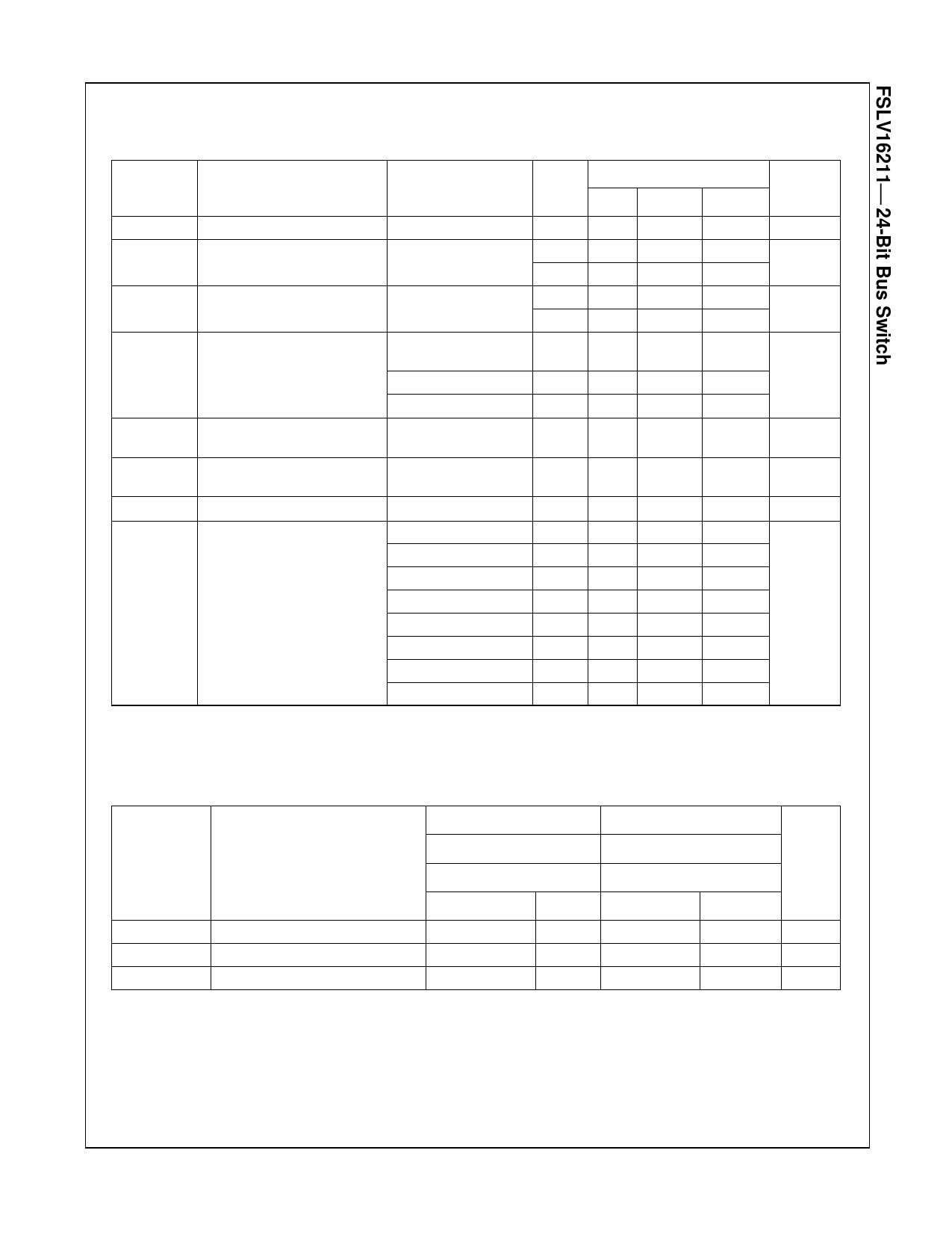
DC Electrical Characteristics
Not all conditions may appear on all switch types.
Symbol
Parameter
VIK
Clamp Diode Voltage
VIH
HIGH Level Control Input
Voltage
VIL
LOW Level Control Input
Voltage
IL
Input Leakage Current
ICC
Quiescent Supply Current
∆ICC
Increase in ICC per Input
IOZ
Off-State Leakage
RON
Switch On Resistance
Conditions
TA = -40°C to +85°C
VCC (V)
Min. Typ. Max.
IIN = -18mA
3.0
-1.2
2.3-2.7 1.7
2.7-3.6 2.0
2.3-2.7
0.7
2.7-3.6
0.8
Force VI = 3.6V,
IOUT = 0.0A
2.3
Force VI = 3.6V
0.0
0 ≤ VIN ≤ 3.6V
3.6
VIN = VCC or GND,
IOUT = 0A
3.6
One Input at 3V Other
Inputs at VCC or GND
3.6
0.0 ≤ A, B ≤ 3.6V
3.6 -1.0
10.0
10.0
1.0
10.0
300.0
1.0
IIN = 64mA, VI = 0.0V 3.0
IIN = 30mA, VI = 0.0V 3.0
IIN = 15mA, VI = 2.4V 3.0
IIN = 15mA, VI = 3.0V 2.3
IIN = 64mA, VI = 0.0V 2.3
IIN = 30mA, VI = 0.0V 2.3
IIN = 15mA, VI = 1.7V 2.3
IIN = 15mA, VI = 2.0V 2.3
5.0
7.0
5.0
7.0
10.0
15.0
20.0
5.0
8.0
5.0
8.0
10.0
15.0
20.0
Units
V
V
V
µA
µA
µA
µA
Ω
AC Electrical Characteristics
TA=-40°C to +85°C
TA=40°C to +85°C
Symbol
Parameter
CL=30pF, RL=500Ω
VCC = 2.5V ± 0.20V
CL=50pF, RL=500Ω
VCC=3.3V ± 0.30V
Units
Min.
Max.
Min.
Max.
tPHL, tPLH
Propagation Delay(3)
0.15
0.25
ns
tPHZ, tPLZ Enable Time
0.5
4.7
1.0
7.0
ns
tPZH, tPZL Disable Time
0.5
5.1
1.0
5.5
ns
Note:
3. This parameter is guaranteed by design, but is not production tested. The bus switch contributes no propagation
delay other than the RC delay of the typical on resistance of the switch and the load capacitance, when driven by
an ideal voltage source (zero output impedance).
© 2003 Fairchild Semiconductor Corporation
FSLV16211 Rev. 1.0.1
4
www.fairchildsemi.com
Share Link: 