UPD75P3018GC-3B9 Ver la hoja de datos (PDF) - NEC => Renesas Technology
Número de pieza
componentes Descripción
Fabricante
UPD75P3018GC-3B9 Datasheet PDF : 60 Pages
| |||
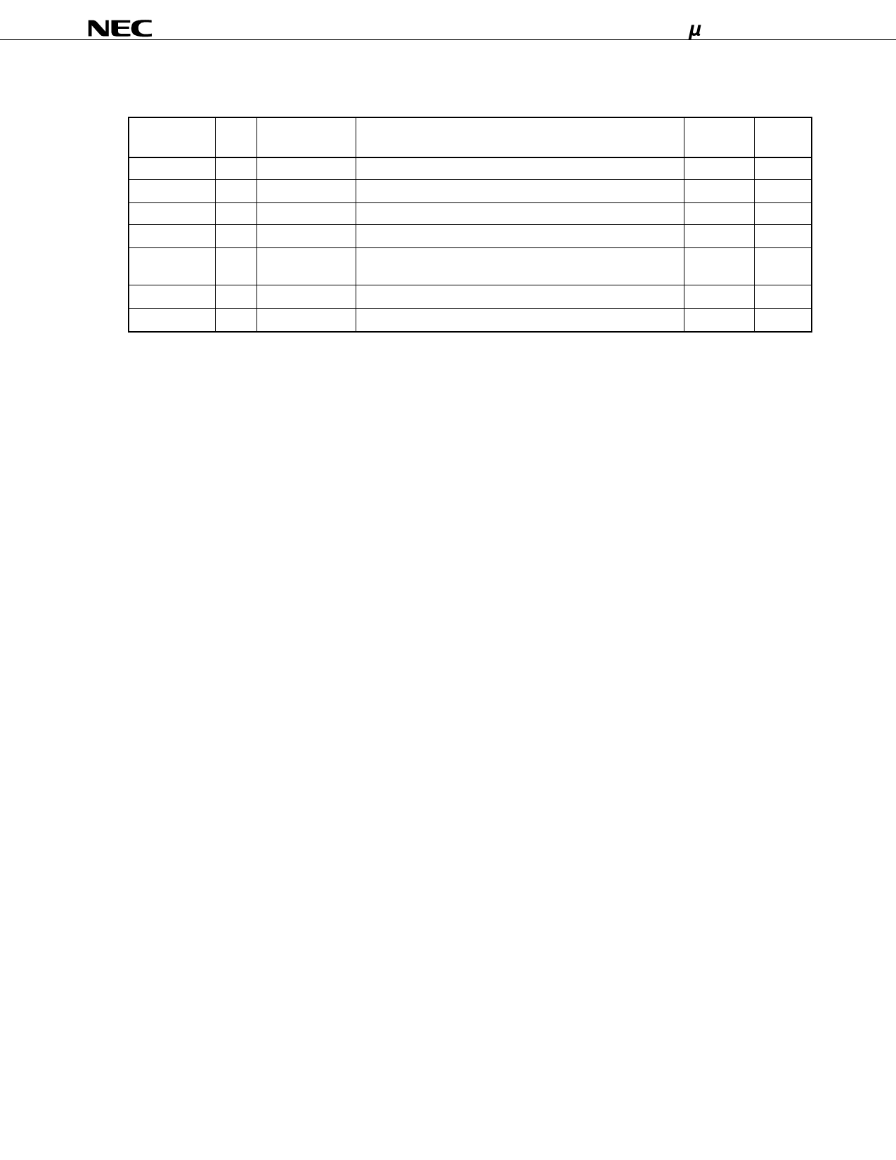
µPD75P3018
3.2 Non-port Pins (2/2)
Pin name
I/O
Shared by
S0-S23
Output
—
S24-S31
Output BP0-BP7
COM0-COM3 Output
—
VLC0-VLC2
—
—
BIAS
Output
—
LCDCLNote 2
SYNCNote 2
I/O P30
I/O P31
Function
Status I/O circuit
after reset type
Segment signal output
Note 1
G-A
Segment signal output
Note 1
H-A
Common signal output
Note 1
G-B
Power source for LCD driver
—
—
Output for external split resistor cut
High
—
impedance
Clock output for driving external expansion driver
Input
E-B
Clock output for synchronization of external expansion driver Input
E-B
Notes 1. The VLCX (X = 0, 1, 2) shown below are selected as the input source for the display outputs.
S0-S31: VLC1, COM0-COM2: VLC2, COM3: VLC0
2. These pins are provided for future system expansion. Currently, only P30 and P31 are used.
9
Share Link: 