FS5AS-10A-T13 Ver la hoja de datos (PDF) - Renesas Electronics
Número de pieza
componentes Descripción
Fabricante
FS5AS-10A-T13 Datasheet PDF : 7 Pages
| |||
FS5AS-10A
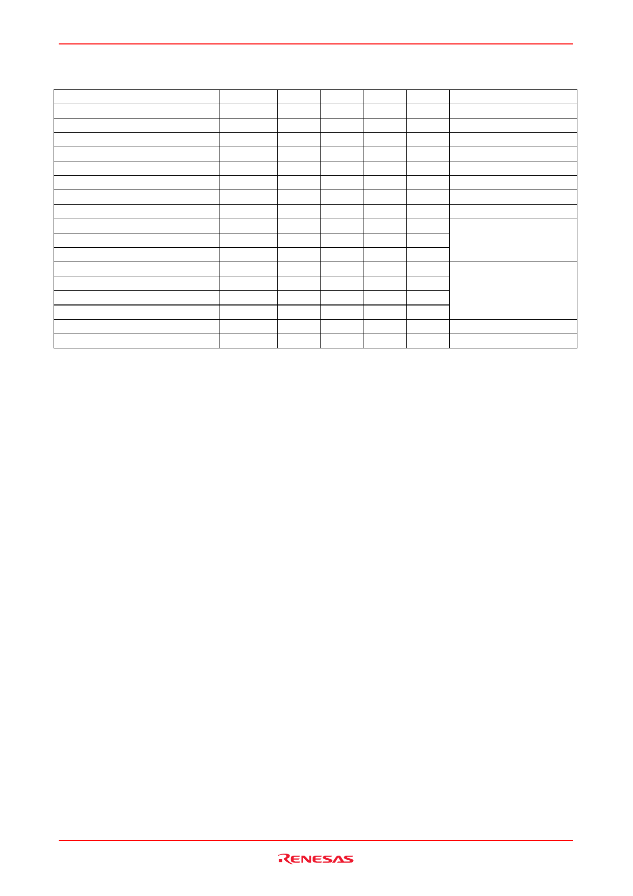
Electrical Characteristics
Parameter
Drain-source breakdown voltage
Gate-source breakdown voltage
Gate-source leakage current
Drain-source leakage current
Gate-source threshold voltage
Drain-source on-state resistance
Drain-source on-state voltage
Forward transfer admittance
Input capacitance
Output capacitance
Reverse transfer capacitance
Turn-on delay time
Rise time
Turn-off delay time
Fall time
Source-drain voltage
Thermal resistance
Symbol
V(BR)DSS
V(BR)GSS
IGSS
IDSS
VGS(th)
rDS(ON)
VDS(ON)
| yfs |
Ciss
Coss
Crss
td(on)
tr
td(off)
tf
VSD
Rth(ch-c)
Min.
500
±30
—
—
2.5
—
—
2.7
—
—
—
—
—
—
—
—
—
Typ.
—
—
—
—
3.0
1.2
2.4
4.5
700
70
15
15
20
90
30
1.5
—
Max.
—
—
±10
1
3.5
1.5
3.0
—
—
—
—
—
—
—
—
2.0
1.92
Unit
V
V
µA
mA
V
Ω
V
S
pF
pF
pF
ns
ns
ns
ns
V
°C/W
(Tch = 25°C)
Test conditions
ID = 1 mA, VGS = 0 V
IG = ±100 µA, VDS = 0 V
VGS = ±25 V, VDS = 0 V
VDS = 500 V, VGS = 0 V
ID = 1 mA, VDS = 10 V
ID = 2 A, VGS = 10 V
ID = 2 A, VGS = 10 V
ID = 2 A, VDS = 10 V
VDS = 25 V, VGS = 10 V,
f = 1MHz
VDD = 200 V, ID = 2 A,
VGS = 10 V,
RGEN = RGS = 50 Ω
IS = 2 A, VGS = 0 V
Channel to case
Rev.1.00, Aug.20.2004, page 2 of 6
Share Link: 