FOD3120 Ver la hoja de datos (PDF) - Fairchild Semiconductor
Número de pieza
componentes Descripción
Fabricante
FOD3120 Datasheet PDF : 22 Pages
| |||
October 2009
FOD3120
High Noise Immunity, 2.5A Output Current,
Gate Drive Optocoupler
Features
■ High noise immunity characterized by 35kV/µs
minimum common mode rejection
■ 2.5A peak output current driving capability for most
1200V/20A IGBT
■ Use of P-channel MOSFETs at output stage enables
output voltage swing close to the supply rail
■ Wide supply voltage range from 15V to 30V
■ Fast switching speed
– 400ns max. propagation delay
– 100ns max. pulse width distortion
■ Under Voltage LockOut (UVLO) with hysteresis
■ Extended industrial temperate range, -40°C to 100°C
temperature range
■ Safety and regulatory approved
– UL1577, 5000 VRMS for 1 min.
– IEC60747-5-2
■ RDS(ON) of 1Ω (typ.) offers lower power
dissipation
■ >8.0mm clearance and creepage distance
(option ‘T’ or ‘TS’)
■ 1,414V Peak Working Insulation Voltage (VIORM)
Applications
■ Industrial inverter
■ Uninterruptible power supply
■ Induction heating
■ Isolated IGBT/Power MOSFET gate drive
Description
The FOD3120 is a 2.5A Output Current Gate Drive
Optocoupler, capable of driving most 1200V/20A
IGBT/MOSFET. It is ideally suited for fast switching
driving of power IGBT and MOSFETs used in motor
control inverter applications, and high performance
power system.
It utilizes Fairchild’s proprietary coplanar packaging
technology, Optoplanar®, and optimized IC design to
achieve high noise immunity, characterized by high
common mode rejection.
It consists of a gallium aluminum arsenide (AlGaAs) light
emitting diode optically coupled to an integrated circuit
with a high-speed driver for push-pull MOSFET output
stage.
Related Resources
■ FOD3150, 1A Output Current, Gate Drive
Optocoupler Datasheet
■ www.fairchildsemi.com/products/opto/
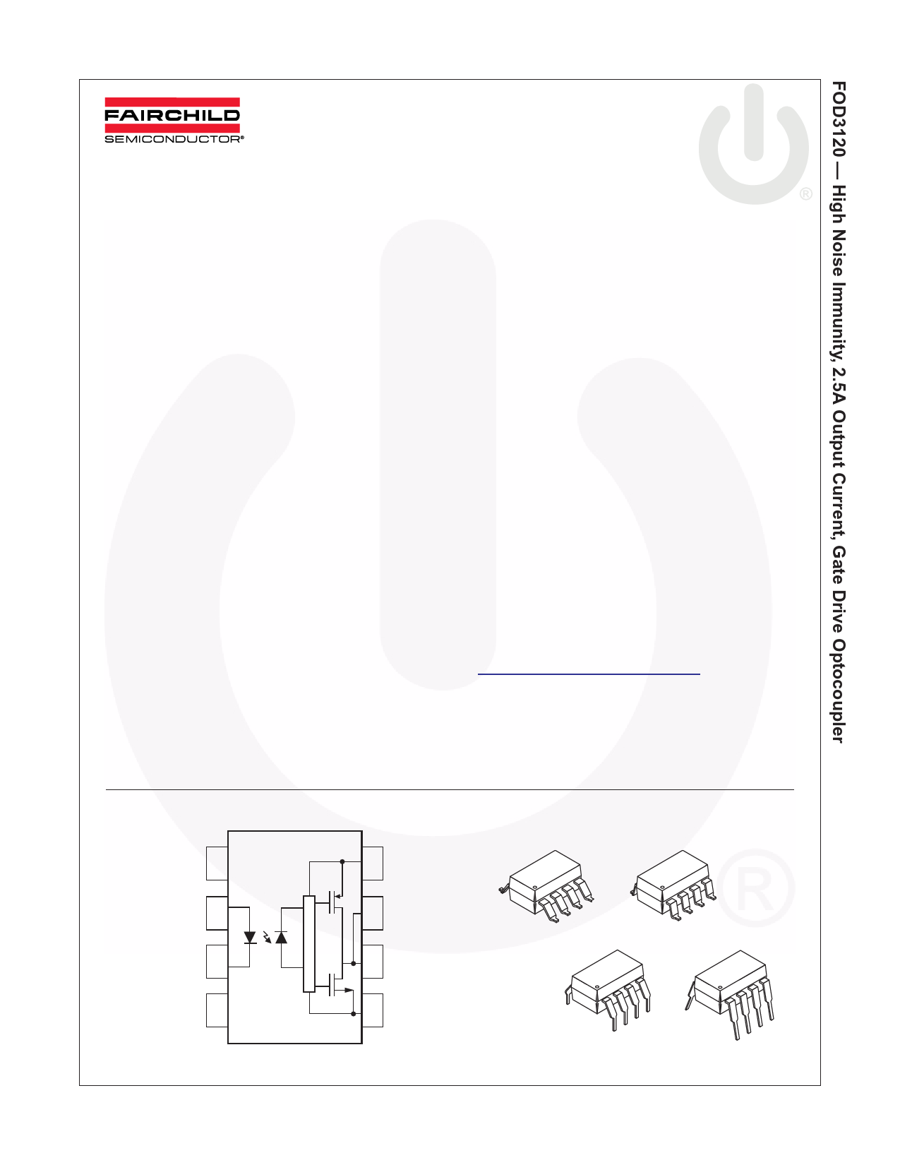
Functional Block Diagram
Package Outlines
NC 1
ANODE 2
8 VCC
8
7 VO2
CATHODE 3
6 VO1
NC 4
5 VEE
Note:
A 0.1µF bypass capacitor must be connected between pins 5 and 8.
©2003 Fairchild Semiconductor Corporation
FOD3120 Rev. 1.17.0
8
1
1
8
1
8
1
www.fairchildsemi.com
Share Link: 