FAN7602C Ver la hoja de datos (PDF) - Fairchild Semiconductor
Número de pieza
componentes Descripción
Fabricante
FAN7602C Datasheet PDF : 19 Pages
| |||
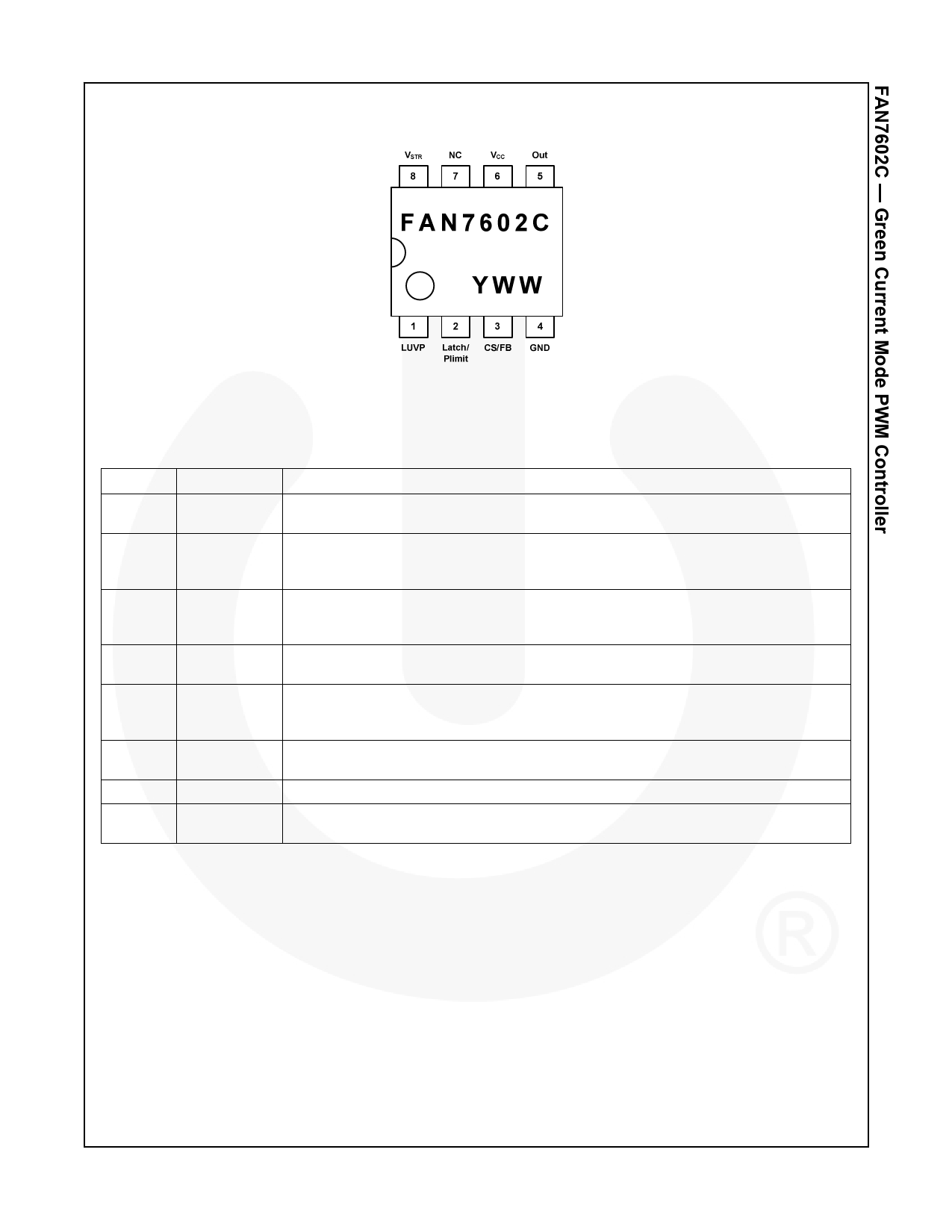
Pin Configuration
Figure 3. Pin Configuration (Top View)
Pin Definitions
Pin #
1
2
3
4
5
6
7
8
Name
LUVP
Latch/Plimit
CS/FB
GND
OUT
VCC
NC
VSTR
Description
Line Under-Voltage Protection Pin. This pin is used to protect the set when the input
voltage is lower than the rated input voltage range.
Latch Protection and Power Limit Pin. When the pin voltage exceeds 4V, the latch
protection works. The latch protection is reset when the VCC voltage is lower than 5V. For
the power limit function, the OCP level decreases as the pin voltage increases.
Current Sense and Feedback Pin. This pin is used to sense the MOSFET current for
the current mode PWM and OCP. The output voltage feedback information and the
current sense information are added using an external RC filter.
Ground Pin. This pin is used for the ground potential of all the pins. For proper operation,
the signal ground and the power ground should be separated.
Gate Drive Output Pin. This pin is an output pin to drive an external MOSFET. The peak
sourcing current is 450mA and the peak sinking current is 600mA. For proper operation,
the stray inductance in the gate driving path must be minimized.
Supply Voltage Pin. IC operating current and MOSFET driving current are supplied
using this pin.
No Connection.
Startup Pin. This pin is used to supply IC operating current during IC startup. After
startup, the internal JFET is turned off to reduce power loss.
© 2009 Fairchild Semiconductor Corporation
FAN7602C • Rev. 1.0.0
3
www.fairchildsemi.com
Share Link: 