FAN7554 Ver la hoja de datos (PDF) - Fairchild Semiconductor
Número de pieza
componentes Descripción
Fabricante
FAN7554 Datasheet PDF : 22 Pages
| |||
FAN7554
S/S
2
100uA
5V
Ds
2R
1mA
R
Cs
Cfb
Output drive
5uA 5V
Vcc
1
FB
FAN7554
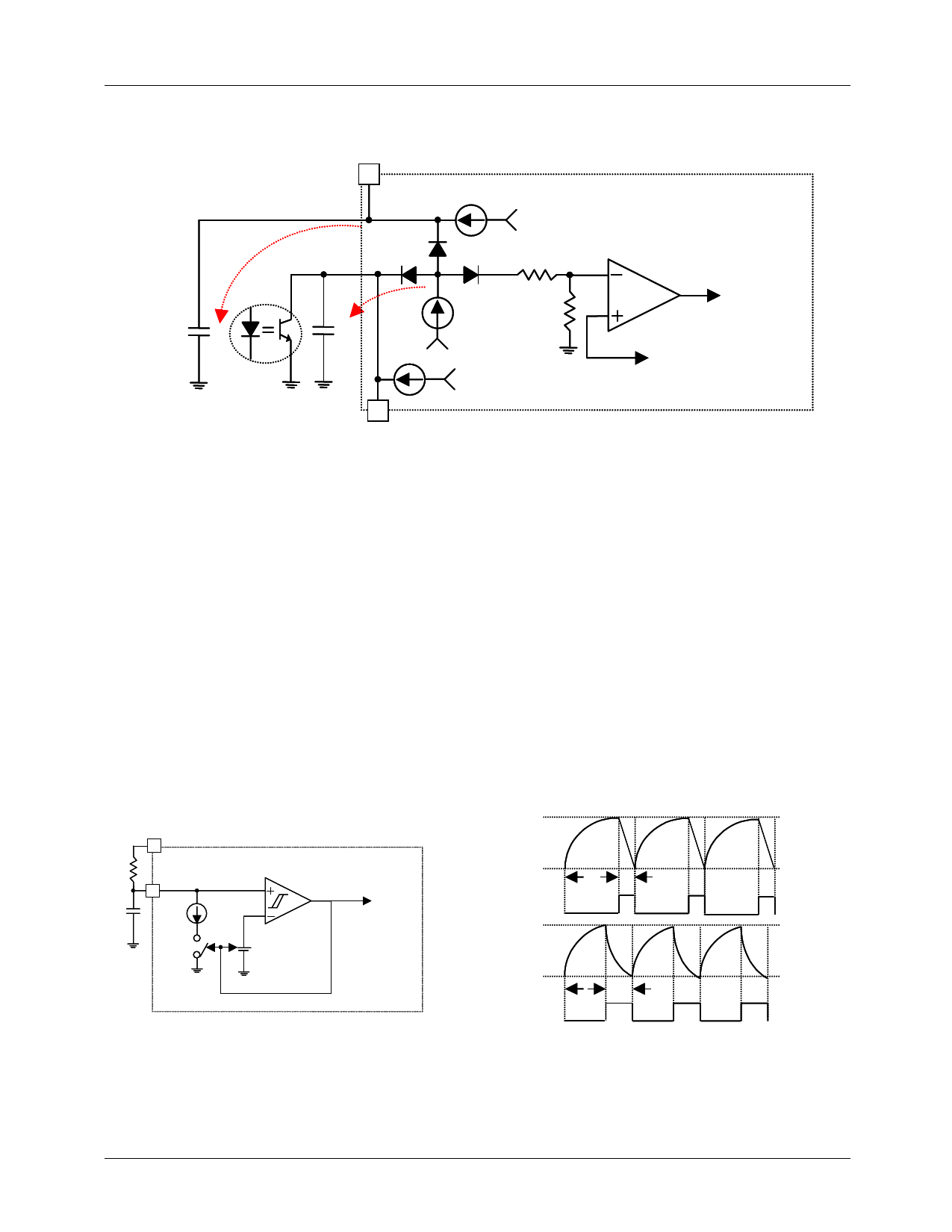
Figure 13. Soft Start Circuit & Circuit Flow
Oscillator
As shown in figure14, the oscillator frequency is programmed by values selected for timing components Rt and Ct. Capacitor
Ct is charged to almost 2.8V through resistor Rt from the 5V reference and discharged to 1.2V by an internal current source.
The oscillator generates the clock signal while the timing capacitor Ct is discharged. The gate drive output becomes low during
the clock time. Rt and Ct selection determine the oscillator frequency and maximum duty cycle. Charge and discharge times
can be calculated through the equations below.
Charging time : tc = 0.55×Rt×Ct
Discharging time : td = Rt×Ct×ln[(0.0063×Rt - 2.8) / (0.0063×Rt - 3.8)]
where the oscillator frequency : fosc = (tc + td)-1 (±10%)
When Rt > 5kΩ, fosc = 1 / (0.55×Rt×Ct) = 1.8 / (Rt×Ct)
Vref
8
Rt
CT
Ct 4
Ct
+
Discharge
-
Discharge
2.8V
/1.2V
Clock
Gate Drive
FAN7554
Figure 14. Oscillator Circuit
Vhigh(2.8V)
Sawtooth waveform
Vlow(1.2V)
tc
td
[ Rt > 5kΩ]
Internal clock
Vhigh(2.8V)
Sawtooth waveform
Vlow(1.2V)
Internal clock
td
tc
[ Rt < 5kΩ]
Figure 15. Sawtooth & Clock Waveform
9
Share Link: 