FAN6921MLMY Ver la hoja de datos (PDF) - Fairchild Semiconductor
Número de pieza
componentes Descripción
Fabricante
FAN6921MLMY
Fairchild Semiconductor

FAN6921MLMY Datasheet PDF : 23 Pages
| |||
Marking Information
16
ZXYTT
FAN6921FO
TPM
1
- Fairchild Logo
Z - Plant Code
X - Year Code (1 Digit for SOP, 2 Digits for DIP)
Y - Week Code (1 Digit for SOP, 2 Digits for DIP)
TT – DIe-Run Code
F - Frequency (M=Low, H=High Level)
O - OLP Mode (L=Latch, R=Recovery)
T - Package Type (N=DIP, M=SOP)
P – Y=Green Package
M - Manufacture Flow Code
Figure 3. Marking Diagram
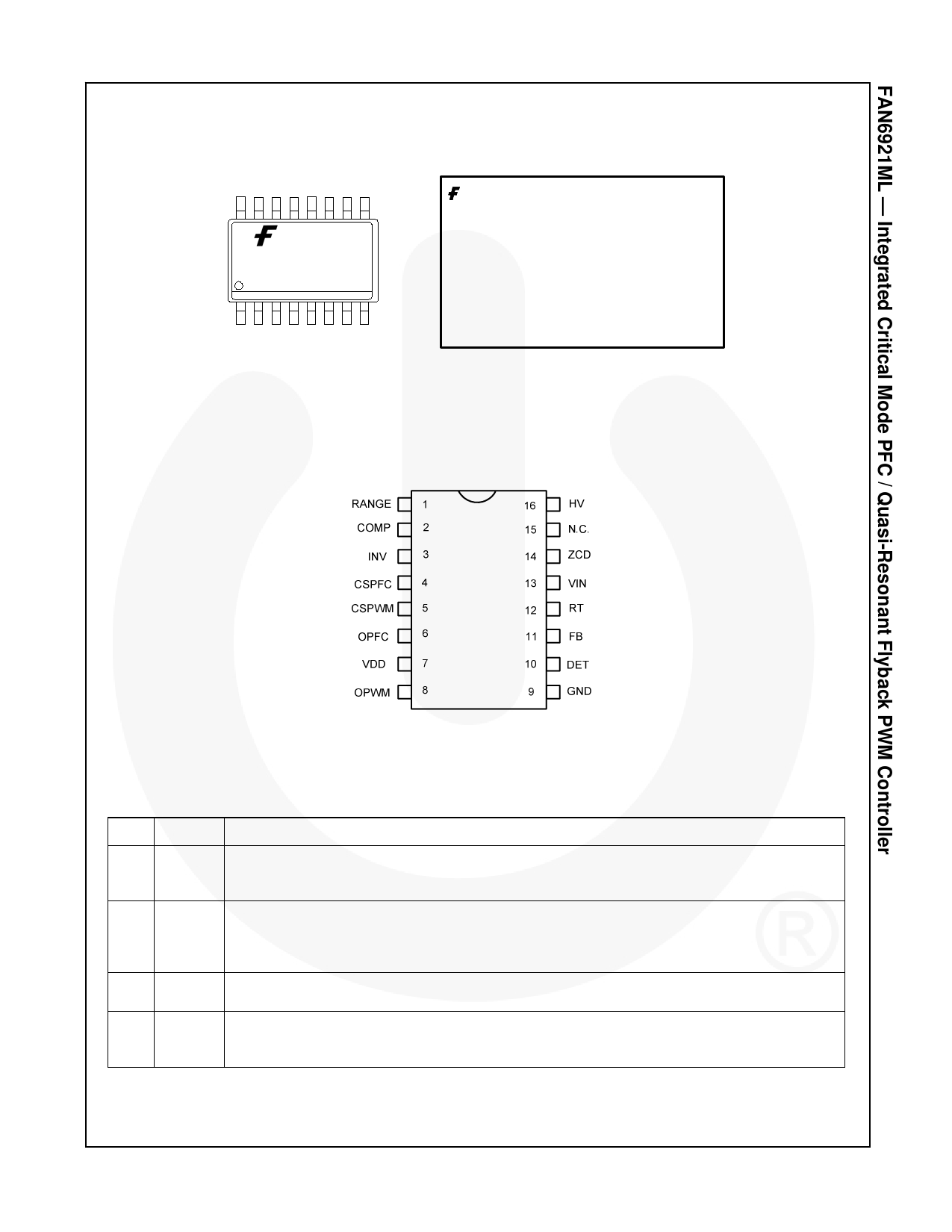
Pin Configuration
Figure 4. Pin Configuration
Pin Definitions
Pin # Name Description
RANGE pin’s impedance changes according to VIN pin voltage level. When the input voltage
1 RANGE detected by the VIN pin is lower than a threshold voltage, it sets to high impedance; whereas it
sets to low impedance if input voltage is high level.
Output pin of the error amplifier. It is a transconductance type error amplifier for PFC output
2
COMP
voltage feedback. Proprietary multi-vector current is built-in to this amplifier; therefore, the
compensation for the PFC voltage feedback loop allows a simple compensation circuit between
this pin and GND.
3
INV
Inverting input of the error amplifier. This pin is used to receive PFC voltage level by a voltage
divider and provides PFC output over- and under-voltage protections.
Input to the PFC over-current protection comparator that provides cycle-by-cycle current limiting
4 CSPFC protection. When the sensed voltage across the PFC current-sensing resistor reaches the internal
threshold (0.6 typical), the PFC switch is turned off to activate cycle-by-cycle current limiting.
© 2010 Fairchild Semiconductor Corporation
FAN6921ML • Rev. 1.0.1
4
www.fairchildsemi.com
Share Link: