FAH4820 Ver la hoja de datos (PDF) - Fairchild Semiconductor
Número de pieza
componentes Descripción
Fabricante
FAH4820 Datasheet PDF : 14 Pages
| |||
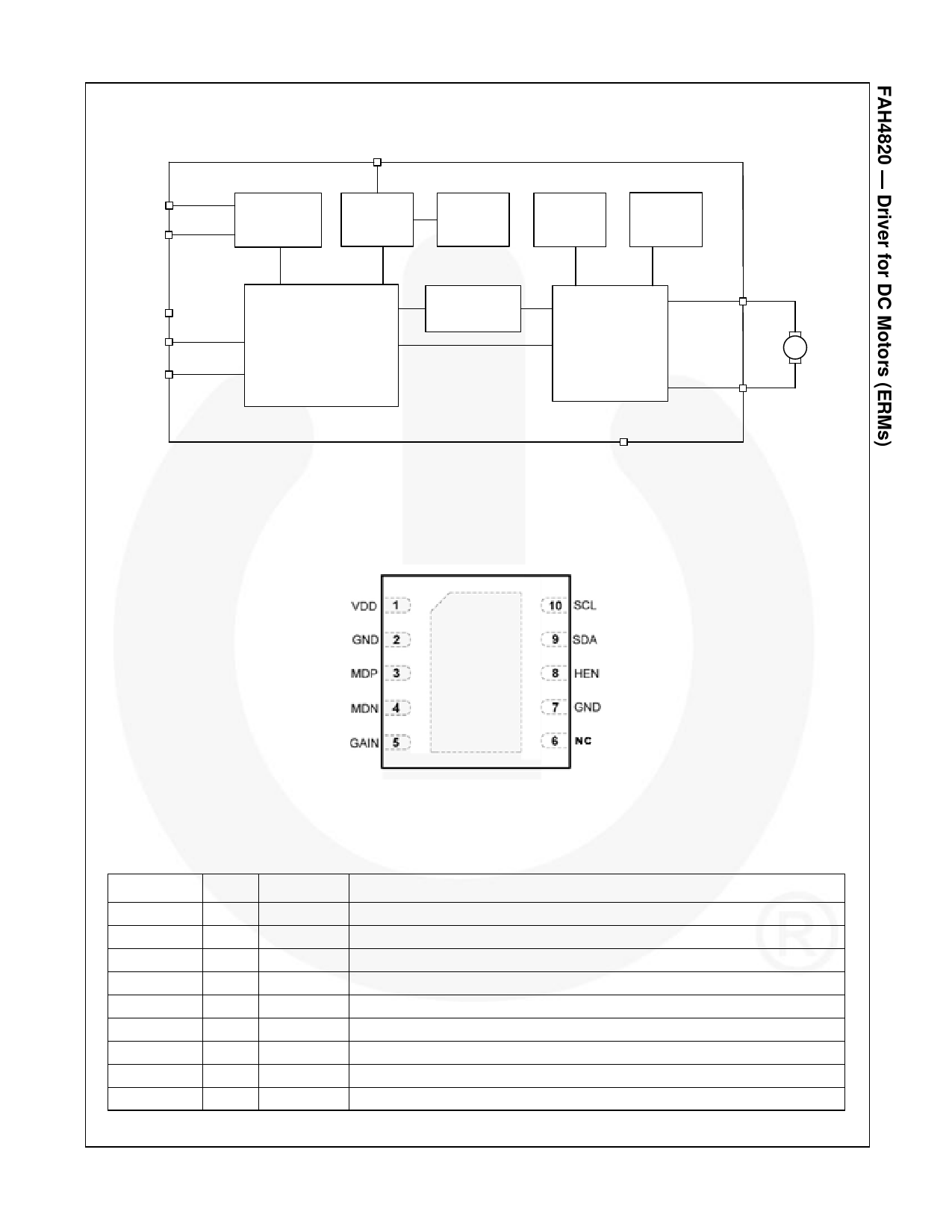
Block Diagram
VDD
SCL
Serial I2C
Interface
Bandgap
Reference
UVLO
OCP
OTP
SDA
Programmable
MDP
LDO
HEN
Control Logic and Register
Differential Driver
GND
MDN
GAIN
Figure 1. Block Diagram
Pin Configuration
Figure 2. Pin Assignments
Pin Definitions
Name Pin #
VDD
1
GND
2, 7
MDP
3
MDN
4
GAIN
5
NC
6
HEN
8
SDA
9
SCL
10
Type
Power
Power
Output
Output
Input
NA
Input
Input
Input
Description
Power
Ground
Positive motor driver output
Negative motor driver output
Gain control for motor driving
No connection
Motor enable/disable (HIGH: enable, LOW: disable)
I2C data input
I2C clock input
© 2013 Fairchild Semiconductor Corporation
FAH4820 • 1.0.0
2
www.fairchildsemi.com
Share Link: 