ESD11N5.0ST5G Ver la hoja de datos (PDF) - ON Semiconductor
Número de pieza
componentes Descripción
Fabricante
ESD11N5.0ST5G Datasheet PDF : 4 Pages
| |||
ESD11N5.0ST5G
ELECTRICAL CHARACTERISTICS
(TA = 25°C unless otherwise noted)
Symbol
Parameter
IPP
Maximum Reverse Peak Pulse Current
VC
Clamping Voltage @ IPP
VRWM Working Peak Reverse Voltage
IR
Maximum Reverse Leakage Current @ VRWM
VBR
Breakdown Voltage @ IT
IT
Test Current
*See Application Note AND8308/D for detailed explanations of
datasheet parameters.
I
IPP
VC VBR VRWM IIRT
IIRT
VRWM VBR VC V
IPP
Bi−Directional TVS
ELECTRICAL CHARACTERISTICS (TA = 25°C unless otherwise noted)
VRWM IR (mA) VBR (V) @ IT
(V) @ VRWM
(Note 2)
IT
Device
Device
Marking Max
Max
Min
mA
ESD11N5.0ST5G
N5S0
5.0
1.0
5.8
1.0
C (pF)
Typ
Max
0.6
0.9
2. VBR is measured with a pulse test current IT at an ambient temperature of 25°C.
3. For test procedure see Figures 3 and 4 and Application Note AND8307/D.
VC
Per IEC61000−4−2
(Note 3)
Figures 1 and 2
See Below
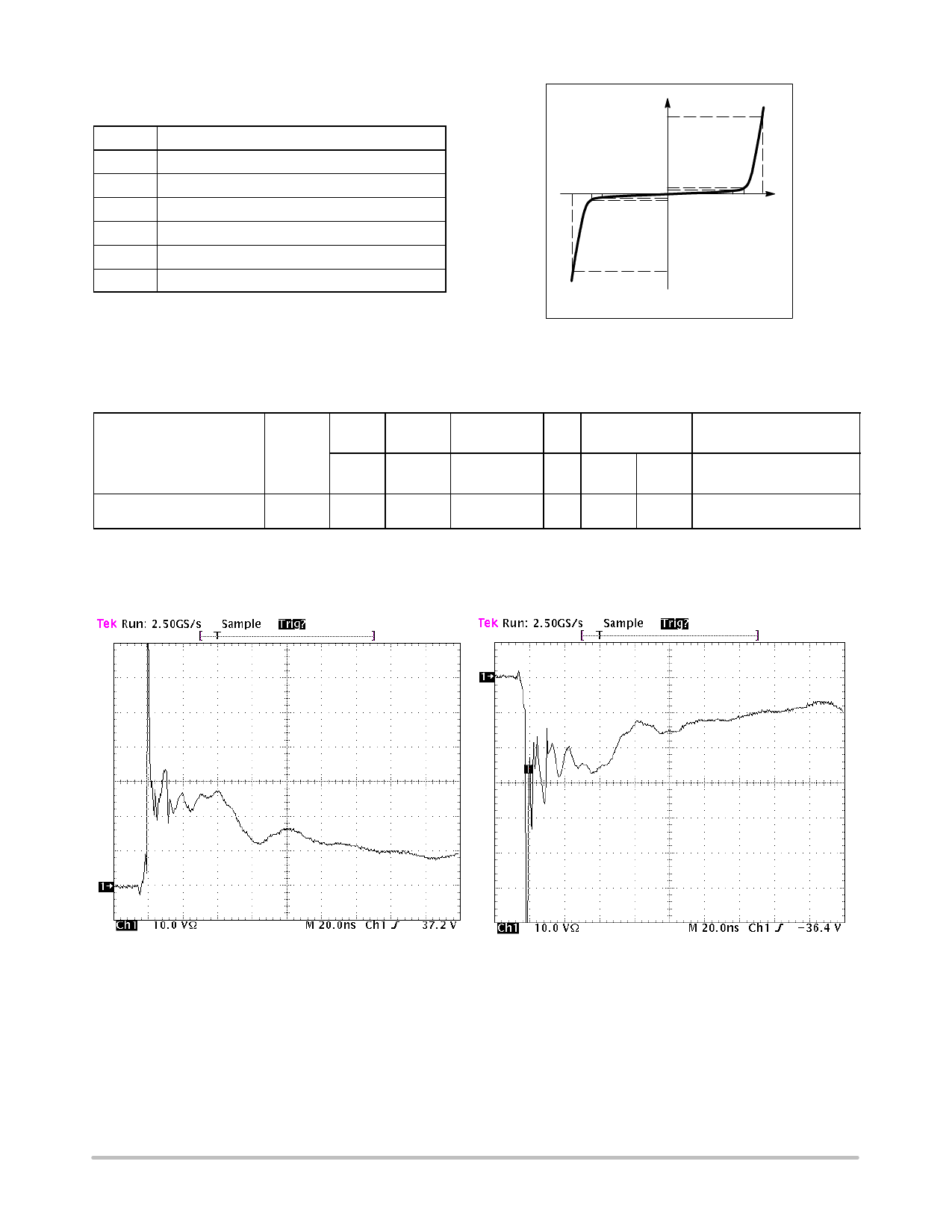
Figure 1. ESD Clamping Voltage Screenshot
Positive 8 kV Contact per IEC61000−4−2
Figure 2. ESD Clamping Voltage Screenshot
Negative 8 kV Contact per IEC61000−4−2
http://onsemi.com
2
Share Link: 