EL2111 Ver la hoja de datos (PDF) - Intersil
Número de pieza
componentes Descripción
Fabricante
EL2111 Datasheet PDF : 6 Pages
| |||
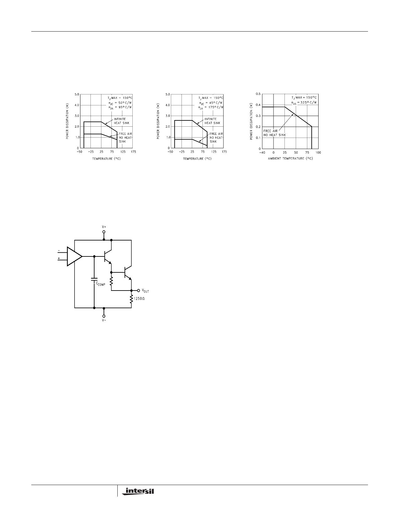
Typical Performance Curves
8-Pin Plastic DIP
Maximum Power Dissipation
vs Ambient Temperature
EL2111
8-Pin SO
Maximum Power Dissipation
vs Ambient Temperature
5-Pin SOT23
Maximum Power Dissipation
vs Ambient Temperature
Simplified Block Diagram
Applications Information
Product Description
The EL2111 operational amplifier is stable at a gain of 1. It is
built on Elantec’s proprietary complimentary bipolar process.
This topology allows it to be used in a variety of applications
where current mode amplifiers are not appropriate because
of restrictions placed on the feedback elements. This product
is especially designed for applications where high bandwidth
and good video performance characteristics are desired but
the higher cost of more flexible and sophisticated products
are prohibitive.
Power Supplies
The EL2111 is designed to work at a supply voltage
difference of 4.5V to 5.5V. It will work on any combination of
4
± supplies. All electrical characteristics are measured with a
5V supply.
Output Swing vs Load
Please refer to the simplified block diagram. This amplifier
provides an NPN pull-up transistor output and a passive
1250Ω pull-down resistor to the most negative supply. In a
application where the load is connected to VS- the output
voltage can swing to within 200mV of VS-.
Output Drive Capability
This device does not have short circuit protection. Each
output is capable of than 100mA into a shorted output. Care
must be used in the design to limit the output current with a
series resistor.
Single 5V Supply Video Cable Driver
These amplifiers may be used as a direct coupled video
cable driver with a gain of 2. With a 75Ω back matching
resistor driving a terminated 75Ω cable the output at the
cable load will be original video level (1V NTSC). The best
operating mode is with direct coupling. The input signal must
be offset to keep the entire signal within the range of the
amplifier. The required offset voltage can be set with a
resistor divider and a bypass capacitor in the video path
(Figure 1). The input DC offset should be between 0.3V and
0.5V. With RA = 68k and RB = 4.7k the input offset will be
0.32V. Since these amplifiers require a DC load at their
outputs it is good design practice to add a 250Ω resistor to
ground directly at the amplifier output. Then if the 75Ω cable
termination resistor were inadvertently removed there would
still be an output signal. The values in Figure 1 give an
output range of 0V to 2.6V.
Output capacitive coupling also has some restrictions. These
amplifiers require a DC load at their outputs. A 75Ω back
Share Link: 