LA4800V Ver la hoja de datos (PDF) - SANYO -> Panasonic
Número de pieza
componentes Descripción
Fabricante
LA4800V Datasheet PDF : 11 Pages
| |||
LA4800V
External Components Description
Components
C1, C2
C3, C4
C5, C4
C6
C8
C9, C10, C11
C12
R1, R2
R3, R4, R5
R6
Recommended value
1 to 4.7 µF
3.3 to 10 µF
4.7 to 10 µF
0.1 to 1 µF
220 µF
0.22 to 0.47 µF
0.1 to 1.0µF
0.5 to 4.3 Ω
100 kΩ
Description
Input coupling capacitors
Reference bias (VREF) decoupling capacitors
Ripple filter capacitors. Increasing the capacitance also increases the distortion and
the supply rise time at turn ON.
Input coupling capacitor for the beep tone. Choose a value that does not attenuate the
beep tone signal.
Supply line coupling capacitor
Oscillation damping capacitors. Film capacitors are recommended.
Mute time setting capacitor. See the description in the Operating Notes.
Beep tone input signal adjustment resistors. Follow the manufactures instructions.
Power amplifier oscillation damping resistors.
Mute OFF pin 16 bias setting resistor. The internal 300 kΩ resistor and this 100 kΩ
resistor together set the mute switch (pin 16) threshold.
Operating Notes
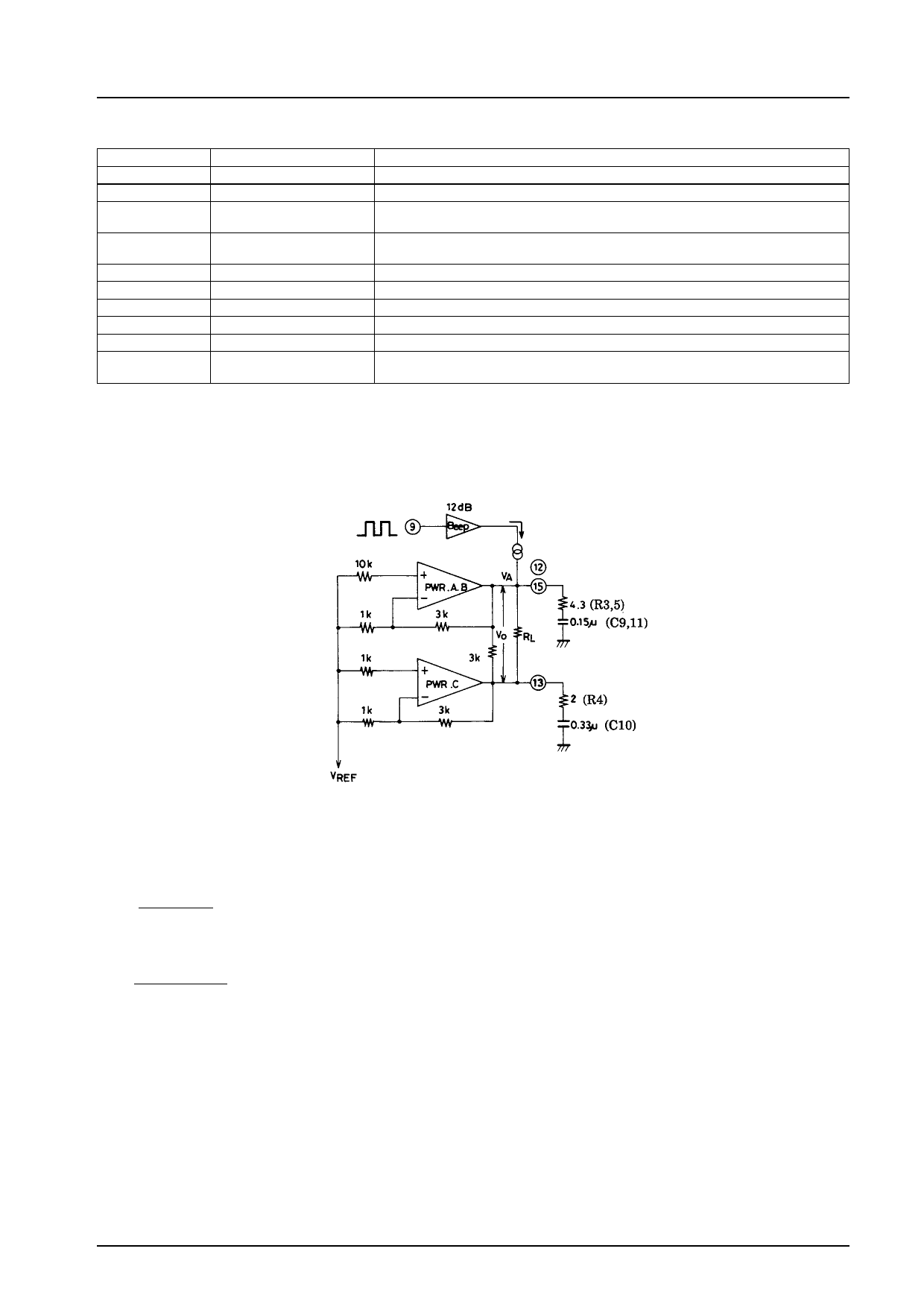
Beep tone operating principle
Signal from microcontroller
Unit (resistance: Ω, capacitance: F)
The design of the above when mute is ON (pin 16 open) is as follows:
The output voltage VO as function of RL is
VO =
RL
× VA
RL+ 3k+ 1k
For example, if RL = 16 Ω and VA = 0.5 V (VA is the adjusted input voltage on pin 9),
16Ω
VO =
× 0.5 ≅ 2 mV
16Ω + 3k+ 1k
The beep tone output voltage VO is determined by the above equation. However, the oscillation damping RC components are
connected to the PWR output and hence these RC components will also influence the actual value of VO. When using the beep
tone, the impedance of C10, connected to the common output (pin 13), must be greater than the impedance of C9 and C11, i.e.
C10 must be greater than C9 and C11.
No.4335-6/11
Share Link: 