RMPA1951-102 Ver la hoja de datos (PDF) - Raytheon Company
Número de pieza
componentes Descripción
Fabricante
RMPA1951-102 Datasheet PDF : 16 Pages
| |||
RF Components
RMPA1951-102
3V PCS CDMA Power Amplifier Module
PRODUCT INFORMATION
DC Power
Management
for Reduced-
Power Operating
Modes
DC Power
Management
Application of Digital
Control Technique
Many Cellular/PCS handsets can benefit from gain control and DC power management to optimize
transmitter performance while operating at backed-off output power levels. Oftentimes, cellular systems
will operate at 10-20 dB back-off from maximum-rated linear power and peak power-added efficiency.
The ability to reduce current consumption under these conditions, without sacrificing linearity, is critical
to extending battery life in next-generation handheld phones.
The RMPA1951-102 PA offers the ability to lower quiescent current by more than 60 percent and small-
signal gain by up to 10 dB using a single control voltage (Vref). Even with the amplifier biased for lowest
current consumption, high linearity is maintained over the full operating temperature range and at output
power levels up to +16 dBm. Bias and gain control through Vref provides complete flexibility for the
handset designer, allowing the user to define the operation by either an analog (continuously-variable)
or digital (discrete-step) voltage input. As an example, reducing the Vref voltage from 2.7V (nominal) to
1.7V (minimum) can lower PA current consumption by more than 20 percent at an output power of +16
dBm.
The following charts demonstrate analog and digital control techniques for minimizing DC power
consumption at reduced RF output power levels. Figures 11 through 19 characterize analog control
over a reference voltage (Vref) range of 1.7V to 2.7V. Quiescent current is reduced to less than 30 mA
and small-signal gain is reduced by 10 dB at Vref=1.7V. Operating current at +16 dBm is also reduced
by 20 percent, or 35 mA, at the lowest reference voltage. Figures 20 through 23 feature digital control
using three discrete voltage levels (2.7V, 2.0V, 1.7V) to optimize linear PA performance over three
output power ranges (< +4 dBm, +4 dBm to +16 dBm, >+16 dBm). Alternate output power ranges can
be selected depending on the power-probability use in the cellular system.
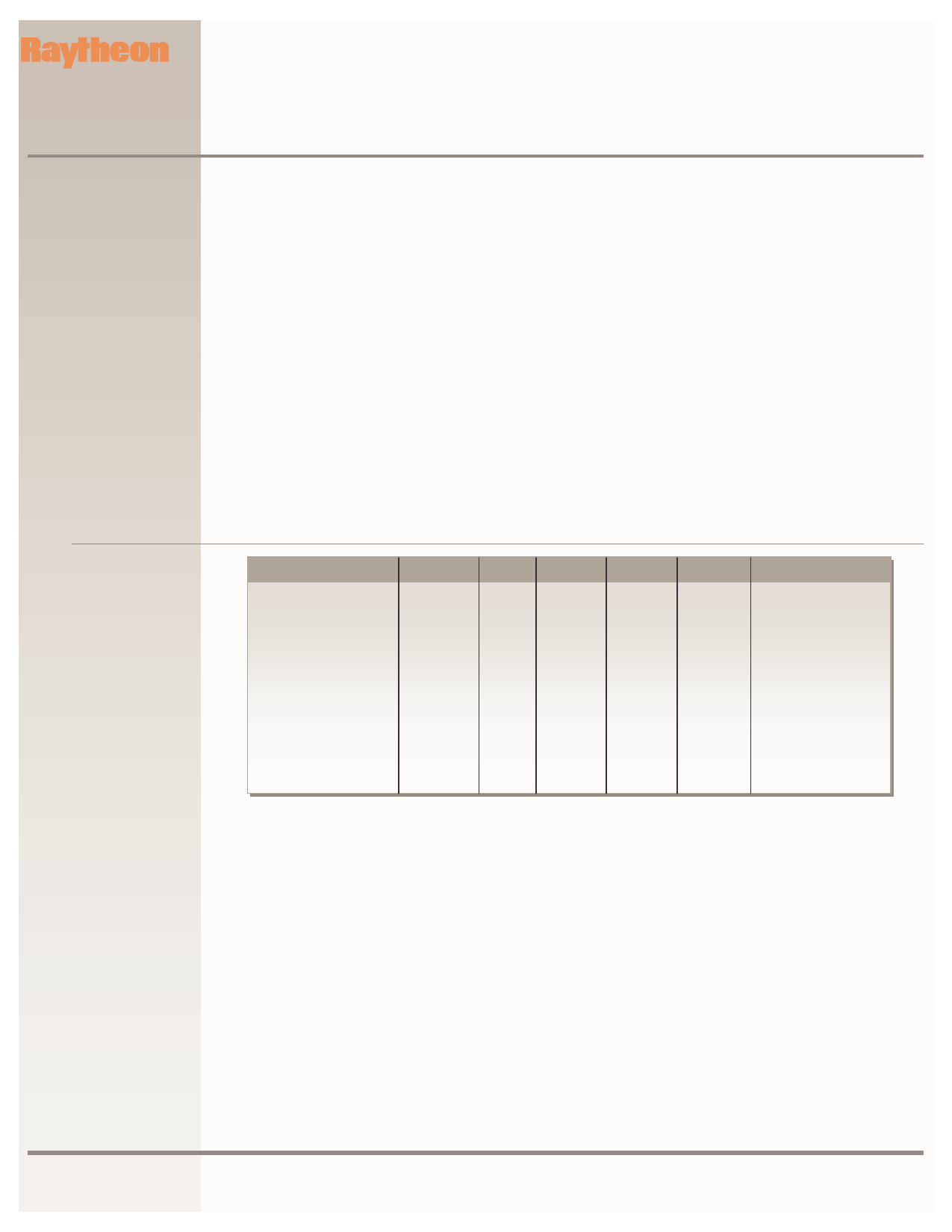
Parameter
Symbol Min Typical
Max
Units Conditions
Low-Power Range
Current
Gain
Linearity
P04
Icc4
G4
ACPR4
+4
dBm Vref=1.7V typ
55
mA
12.5
dB
-50
dBc
Mid-Power Range
P16
+4
+10
Current
Icc16
Gain
G16
20
Linearity
ACPR16
-50
+16
dBm Vref=2.0V typ
160
mA
dB
dBc
High-Power Range
P28
+16
Current
Icc28
560
Gain
G28
26
Linearity
ACPR28
-50
+28
dBm Vref=2.7V typ
640
mA Pout=+28 dBm
dB
dBc
www.raytheonrf.com
Specifications are based on most current or latest revision.
Revised February 6, 2003
Page 9
Raytheon RF Components
362 Lowell Street
Andover, MA 01810
Share Link: 