TQ5122 Ver la hoja de datos (PDF) - TriQuint Semiconductor
Número de pieza
componentes Descripción
Fabricante
TQ5122 Datasheet PDF : 9 Pages
| |||
Measuring the LO Frequency Response
The frequency response of the LO driver amplifier can be
measured using a semi-rigid probe, see Figure 3, and a network
analyzer.
Connect port 1 to the LO input (Pin 4) of the TQ5122 with the
source power set to deliver -7 dBm. Connect the coaxial probe
to Port 2 and place the probe tip approximately 0.1 inch away
from either Pin 3 or the inductor.
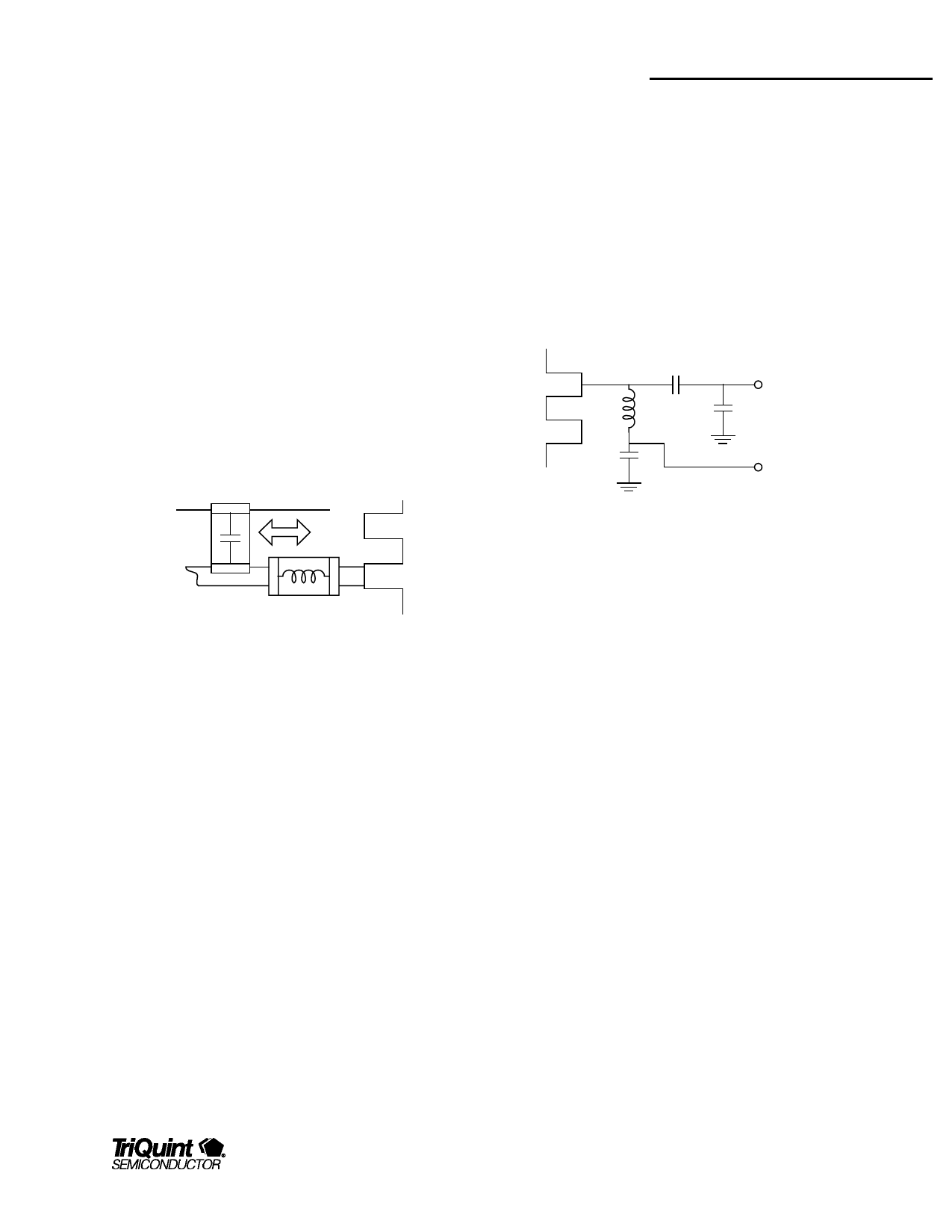
If the calculated shunt inductor (L2) is not a standard value, the
AC ground bypass capacitor C3 can be positioned along the
transmission line to adjust for the right inductance, see Figure 4.
Once this is completed, the peak of the response should be
centered at the center of the LO frequency band.
Placement of C3 will adjust between standard values of
GND
inductors.
Pin 2
C3
Pin 3
L2
Figure 4, Adjusting the AC Ground
TQ5122
Data Sheet
topology must contain either an RF choke or shunt inductor. An
extra DC blocking capacitor is not necessary if the output will be
attached directly to a SAW or crystal bandpass filters.
Figure 5 illustrates a shunt L, series C, shunt C IF matching
network. It is one of the simplest matching networks and
requires the fewest components. DC current can be easily
injected through the shunt inductor and the series C provides a
DC block, if needed. The shunt C, is used to reduce the LO
leakage.
Pin 14
Pin 13
1000pF
10 pF
150nH
IF out
8.2pF
V IF
Figure 5, IF Output Match, 135 MHz
Power down, “sleep” mode
The power down circuit is used to reduce average power
consumption in TDMA applications by toggling the receiver on
and off within the receive time slot when no signal is present.
Mixer IF Port
The Mixer IF output is an "open-drain" configuration, allowing for
flexibility in efficient matching to various filter types and at
various IF frequencies.
For evaluation of the LNA and mixer, it is usually necessary to
impedance match the IF port to the 50Ω test systems. When
verifying or adjusting the matching circuit on the prototype circuit
board, the LO drive should be injected at pin 4 at the nominal
power level of -4 dBm, since the LO level does have an impact
on the IF port impedance.
There are several networks that can be used to properly match
the IF port to the SAW or crystal IF filter. The mixer supply
voltage is applied through the IF port, so the matching circuit
The power down circuitry operates through the incorporation of
enhancement-mode FET switches in all DC paths. Level
shifting circuitry is incorporated for the purpose of providing an
interface compatible with CMOS logic levels. The entire chip
nominally draws 100uA when the power-down pin is at 0V.
When the power-down pin is at 2.8V (Vdd), the chip draws
nominal specified current. The power-down pin itself, Pin 9,
draws approximately 40uA when 2.8V is applied. Less than 1uA
is sourced from the power-down pin when 0V is applied.
For additional information and latest specifications, see our website: www.triquint.com
7
Share Link: 