TQ5122 Ver la hoja de datos (PDF) - TriQuint Semiconductor
Número de pieza
componentes Descripción
Fabricante
TQ5122 Datasheet PDF : 9 Pages
| |||
TQ5122
Data Sheet
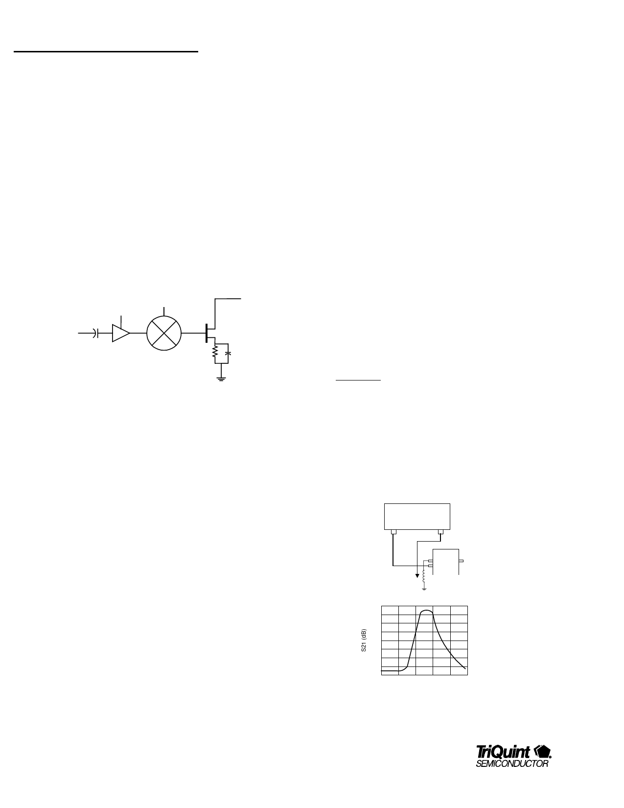
Mixer
The mixer of the TQ5122 uses a common source depletion
mode MESFET. The mixer is designed to operate on supply
voltages from 2.7V to 5V. A 50Ω matched on-chip buffer
amplifier allows direct connection of the LO input to
commercially available VCO’s with output drive levels down to
-7dBm. The common-gate LO buffer provides good input match
and supplies the voltage gain needed to drive the mixer FET.
The mixer also has an "open-drain" IF output which provides
flexibility in matching to various IF frequencies and filter
impedances, see Figure 2.
LO Input
LO Bias Mixer RF
and
Input
Tuning
Open Drain
IF Output
Figure 2, Mixer Section
LO Input Port
The LO input port is matched to 50Ω. This allows the TQ5122
to operate at low LO drivel levels. However, the values and
positions of L2 and C3 shown in the applications circuit effect
the gain of the LO buffer amplifier and are important to the
proper operation of the TQ5122. See “Calculation of nominal L2
Value” below
The common gate buffer amplifier provides the voltage gain
needed to drive the gate of the mixer FET while using very little
current (approximately 1.5mA).
Because of the 50Ω input match of the buffer amplifier and the
internal DC blocking capacitor, the system VCO output can be
directly connected to the TQ5122 LO input via a 50Ω
transmission line with no additional components.
Mixer Input
Although the mixer input port is matched to 50Ω, TriQuint has
found that LO leakage through the Mixer RF input pin, can in
some cases, reflect off the SAW image reject filter and return
back to the mixer out of phase. This may cause some
degradation in conversion gain and system noise figure.
Sensitivity to the phenomena depends on the particular filter
model and the line length between the mixer input pin and the
filter. In some cases a small inductance can be added between
the filter and the mixer input to compensate. With some line
lengths and filter combinations, no inductor is necessary.
LO Buffer & Calculation of Nominal L2 Value
The node between the LO buffer amplifier and the mixer FET is
brought out to Pin 3 (V MX) and connected by an inductor to AC
ground. This inductor is selected to resonate with internal on
chip capacitance at the LO frequency in order to reduce out-of-
band gain and improve noise performance.
The internal capacitance of the LO amplifier output plus the
stray capacitance on the board surrounding Pin 3 is
approximately 1.5 pF. The inductor is selected to resonate with
the total capacitance at the LO frequency using the following
equation:
L
=
1
C(2Πf
)2
, where ⋅ C
=
1.5 pF
The final values must be confirmed with measurements on a
board approximating the final layout. The final layout will affect
the value and position of L2 and its bypass capacitor, C3, see
Figure 5.
Network
Analyzer
Port 1 Port 2
Probe
3
4
TQ5122
-30
-32
-34
-36
-38
-40
-42
700 800 900 1000 1100 1200
Frequency (MHz)
Figure 3. LO Buffer Frequency Response
6
For additional information and latest specifications, see our website: www.triquint.com
Share Link: 