RF2352 Ver la hoja de datos (PDF) - RF Micro Devices
Número de pieza
componentes Descripción
Fabricante
RF2352 Datasheet PDF : 6 Pages
| |||
RF2352
Preliminary
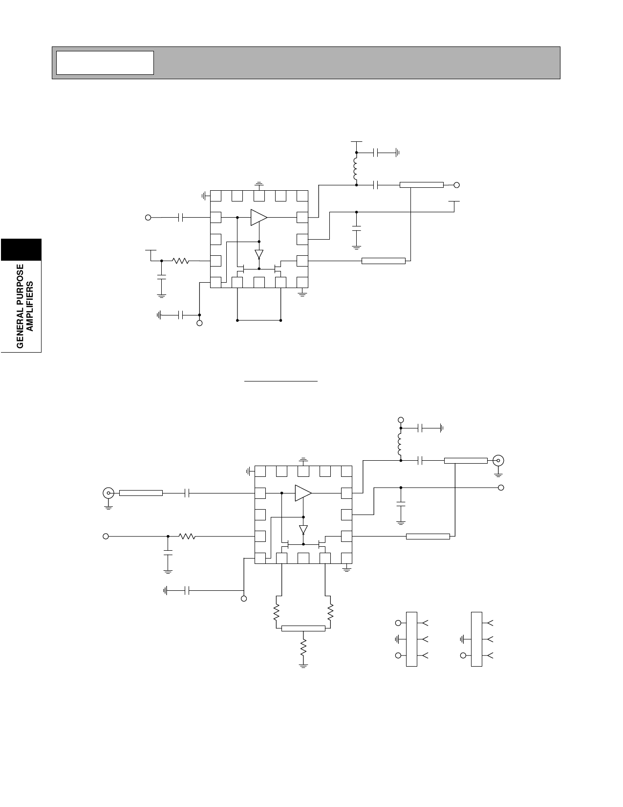
Application Schematic
VCC 1 nF
10 nH
4 pF
50 Ω µstrip
RF OUT
1 16 15 14 13
VCC
22 nF
RF IN
2
12
1 nF
3
11
4
VCC
1500 Ω
50 Ω µstrip
4
10
1 nF
56789
1 nF
MODE SELECT
Package base serves as die flag ground. The vias
connecting the backside of the board should be
large in diameter to allow for easier soldering.
Evaluation Board Schematic
(Download Bill of Materials from www.rfmd.com.)
VCC
J1
RF IN
VREF
50 Ω µstrip
C1
22 nF
R1
1500 Ω
C2
1 nF
C3
1 nF
1 16 15 14 13
2
12
3
11
L1
10 nH
C6
1 nF
C5
4 pF
C4
1 nF
50 Ω µstrip
4
10
56789
2352400-
50 Ω µstrip
J2
RF OUT
VCC
PD R2*
R4*
0Ω
50 Ω µstrip
0Ω
* R2, R3 and R4 form a "Tee" attenuator network which
determines the gain in the bypass mode. Evaluation
boards are shipped with R2 and R4 as 0 Ω jumpers, and
R3 omitted. This configuration provides the maximum
gain (about -4 dB) available in bypass mode.
Package base serves as die flag ground. The vias
connecting the backside of the board should be large in
diameter to allow for easier soldering.
R3*
*
OMIT
P1
1
PD
2 GND
3 VREF
CON3
P2
1
NC
2 GND
3 VCC
CON3
4-180
Rev A4 010720
Share Link: 