TA2022 Ver la hoja de datos (PDF) - Tripath Technology Inc.
Número de pieza
componentes Descripción
Fabricante
TA2022
Tripath Technology Inc.

TA2022 Datasheet PDF : 31 Pages
| |||
Tripath Technology, Inc. - Technical Information
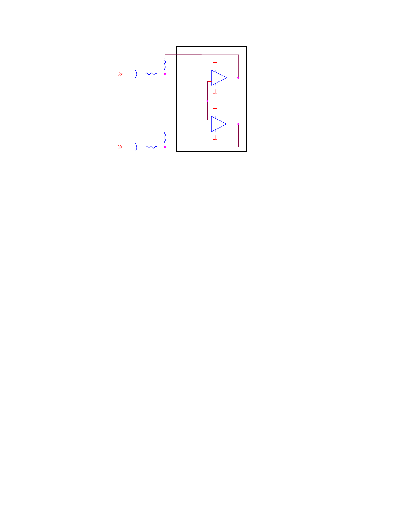
INPUT1
INPUT2
RF
CI
RI
RF
CI
RI
OAOUT1
INV1
TA2022
2
V5
-
+
BIASCAP
INV2
OAOUT2
AGND
V5
+
-
AGND
Figure 1: Input Stage
The gain of the input stage, above the low frequency high pass filter point, is that of a simple inverting
amplifier: It should be noted that the input opamps are biased at approximately 2.5VDC. Thus, the
polarity of CI must be followed as shown in Figure 1 for a standard ground referenced input signal
A VINPUTSTAG E = − R F
RI
Input Capacitor Selection
CI can be calculated once a value for RI has been determined. CI and RI determine the input low
frequency pole. Typically this pole is set below 10Hz. CI is calculated according to:
CI= 1
2π fP R I
where:
RI = Input resistor value in ohms.
fP = Input low frequency pole (typically 10Hz or below).
Modulator Feedback Design
The modulator converts the signal from the input stage to the high-voltage output signal. The
optimum gain of the modulator is determined from the maximum allowable feedback level for the
modulator and maximum supply voltages for the power stage. Depending on the maximum supply
voltage, the feedback ratio will need to be adjusted to maximize performance. The values of RFBA,
RFBB and RFBC (see explanation below) define the gain of the modulator. Once these values are
chosen, based on the maximum supply voltage, the gain of the modulator will be fixed even with as
the supply voltage fluctuates due to current draw.
For the best signal-to-noise ratio and lowest distortion, the maximum modulator feedback voltage
should be approximately 4Vpp. This will keep the gain of the modulator as low as possible and still
allow headroom so that the feedback signal does not clip the modulator feedback stage.
Figure 2 shows how the feedback from the output of the amplifier is returned to the input of the
modulator. The input to the modulator (FBKOUT1/FBKGND1 for channel 1) can be viewed as inputs
to an inverting differential amplifier. RFBA and RFBB bias the feedback signal to approximately 2.5V and
RFBC scales the large OUT1/OUT2 signal to down to 4Vpp.
16
TA2022 – KLI/1.2/07-04
Share Link: