DTA115TSA Ver la hoja de datos (PDF) - ROHM Semiconductor
Número de pieza
componentes Descripción
Fabricante
DTA115TSA Datasheet PDF : 2 Pages
| |||
Transistors
DTA115TH / DTA115TE / DTA115TUA /
DTA115TKA / DTA115TSA
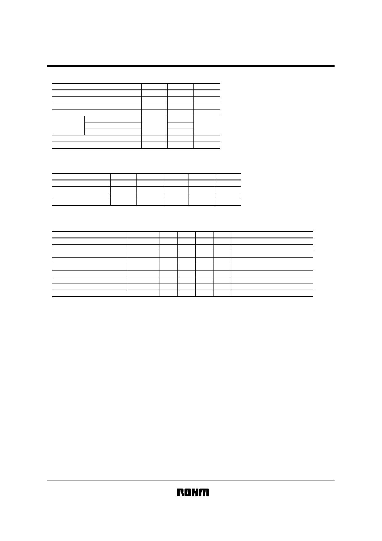
!Absolute maximum ratings (Ta = 25°C)
Parameter
Collector-base voltage
Collector-emitter voltage
Emitter-base voltage
Collector current
Collector power
dissipation
DTA115TH / DTA115TE
DTA115TUA / DTA115TKA
DTA115TSA
Junction temperature
Storage temperature
Symbol
VCBO
VCEO
VEBO
IC
PC
Tj
Tstg
Limits
−50
−50
−5
−100
150
200
300
150
−55 ~ +150
Unit
V
V
V
mA
mW
°C
°C
!Package, marking, and packaging specifications
Part No.
Package
Marking
Packaging code
Basic ordering unit (pieces)
DTA115TH
EMT3H
99
T2L
8000
DTA115TE DTA115TUA DTA115TKA DTA115TSA
EMT3
UMT3
SMT3
SPT
99
99
99
−
TL
T106
T146
TP
3000
3000
3000
5000
!Electrical characteristics (Ta = 25°C)
Parameter
Collector-base breakdown voltage
Collector-emitter breakdown voltage
Emitter-base breakdown voltage
Collector cutoff current
Emitter cutoff current
Collector-emitter saturation voltage
DC current transfer ratio
Input resistance
Transition frequency
∗Transition frequency of the device.
Symbol
BVCBO
BVCEO
BVEBO
ICBO
IEBO
VCE(sat)
hFE
R1
fT
Min. Typ. Max. Unit
Conditions
−50
−
−
V IC=−50µA
−50
−
−
V IC=−1mA
−5
−
−
V IE=−50µA
−
−
−0.5
µA VCB=−50V
−
−
−0.5
µA VEB=−4V
−
−
−0.3
V IC/IB=−1mA/−0.1mA
100
250
600
−
IC=−1mA , VCE=−5V
70
100
130
kΩ
−
−
250
−
MHZ VCE=−10V , IE=5mA , f=100MHZ
∗
Share Link: 