DS7505(2015) Ver la hoja de datos (PDF) - Maxim Integrated
Número de pieza
componentes Descripción
Fabricante
DS7505 Datasheet PDF : 14 Pages
| |||
DS7505
Digital Thermometer and Thermostat
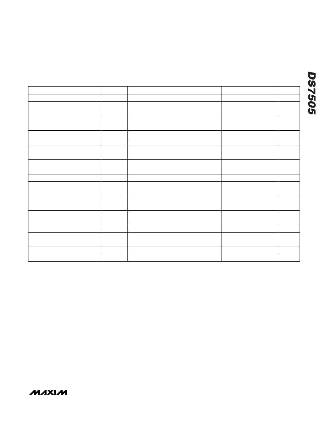
AC Electrical Characteristics (continued)
(1.7V ≤ VDD ≤ 3.7V, TA = -55°C to +125°C, unless otherwise noted.)
PARAMETER
SYMBOL
CONDITIONS
MIN TYP MAX UNITS
EEPROM Data Retention
tEEDR -40°C to +125°C (Note 8)
10
Bus Free Time Between a STOP
and START Condition
tBUF
(Note 9)
1.3
Years
µs
START and Repeated START Hold
Time from Falling SCL
tHD:STA (Notes 9, 10)
600
ns
Low Period of SCL
High Period of SCL
Repeated START Condition Setup
Time to Rising SCL
tLOW
tHIGH
tSU:STA
(Note 9)
(Note 9)
(Note 9)
1.3
µs
0.6
µs
600
ns
Data-Out Hold Time from Falling
SCL
tHD:DAT (Notes 9, 11)
0
0.9
µs
Data-In Setup Time to Rising SCL
Rise Time of SDA and SCL
(Receive)
tSU:DAT
tR
(Note 9)
(Notes 9, 12)
100
ns
1000
ns
Fall Time of SDA and SCL
(Receive)
tF
(Notes 9, 12)
300
ns
Spike Suppression Filter Time
(Deglitch Filter)
tSS
0
50
ns
STOP Setup Time to Rising SCL
Capacitive Load for Each Bus Line
Input Capacitance
Serial Interface Reset Time
tSU:STO
CB
CI
tTIMEOUT
(Note 9)
SDA time low (Note 12)
600
ns
400
pF
5
pF
75
325
ms
Note 1: All voltages are referenced to ground.
Note 2: Internal heating caused by O.S. loading causes the DS7505 to read approximately 0.5°C higher if O.S. is sinking the max-
rated current.
Note 3: Specified in 12-bit conversion mode. Quantization error must be considered when converting in lower resolutions.
Note 4:
Note 5:
Note 6:
Note 7:
Note 8:
IDD specified with O.S. pin open.
IDD specified with VDD at 3.0V and SDA, SCL = 3.0V, TA = -55°C to +85°C.
IDD specified with A0, A1, A2 = 0V or VDD.
VDD must be > 2.0V.
E2 Copy occurs at +25°C.
Note 9: See the timing diagram (Figure 1). All timing is referenced to 0.9 x VDD and 0.1 x VDD.
Note 10: After this period, the first clock pulse is generated.
Note 11: The DS7505 provides an internal hold time of at least 75ns on the SDA signal to bridge the undefined region of SCL’s fall-
ing edge.
Note 12: This timeout applies only when the DS7505 is holding SDA low. Other devices can hold SDA low indefinitely and the
DS7505 does not reset.
www.maximintegrated.com
Maxim Integrated │ 3
Share Link: 