DN3135N8 Ver la hoja de datos (PDF) - Supertex Inc
Número de pieza
componentes Descripción
Fabricante
DN3135N8 Datasheet PDF : 4 Pages
| |||
DN3135
Thermal Characteristics
Package
TO-236AB
ID
(continuous)1
720mA
ID
(pulsed)
300mA
Power Dissipation
@TA = 25OC
0.36W
Θjc (OC/W)
200
Θja (OC/W)
350
TO-243AA
135mA
300mA
1.3W2
34
972
Notes:
1. I (continuous) is limited by max rated T .
D
j
2. Mounted on FR4 board, 25mm x 25mm x 1.57mm. Significant PD increase possible on ceramic substrate.
IDR1
72mA
135mA
IDRM
300mA
300mA
Electrical Characteristics
Symbol Parameter
Min
Typ
Max
Units Conditions
BVDSX Drain-to-source breakdown voltage
350
-
-
V
VGS = -5.0V, ID = 100µA
VGS(OFF) Gate-to-source OFF voltage
-1.5
-
-3.5
V
VDS = 15V, ID = 10µA
ΔVGS(OFF) Change in VGS(OFF) with temperature
-
-
4.5
mV/OC VDS = 15V, ID = 10µA
IGSS Gate body leakage current
-
-
100
nA VGS = ±20V, VDS = 0V
ID(OFF) Drain-to-source leakage current
-
-
1.0
µA VDS = Max rating, VGS = -5.0V
-
-
1.0
mA
VDS = 0.8 Max Rating,
VGS = -5.0V, TA = 125OC
IDSS Saturated drain-to-source current
180
-
-
mA VGS = 0V, VDS = 15V
RDS(ON)
Static drain-to-source ON-state
resistance
-
-
35
Ω
VGS = 0V, ID = 150mA
ΔRDS(ON) Change in RDS(ON) with temperature
-
-
1.1
%/OC VGS = 0V, ID = 150mA
GFS Forward transconductance
140
-
-
mmho VDS = 10V, ID = 100mA
CISS
COSS
CRSS
Input capacitance
Common source output capacitance
Reverse transfer capacitance
-
60
120
VGS = -5.0V,
-
6.0
15
pF VDS = 25V,
-
1.0
10
f = 1MHz
td(ON)
tr
td(OFF)
tf
Turn-ON delay time
Rise time
Turn-OFF delay time
Fall time
-
-
-
-
10
-
15
-
15
VDD = 25V,
ns
ID = 150mA,
RGEN = 25Ω,
-
-
20
VGS = 0v to -10V
VSD Diode forward voltage drop
-
-
1.8
V
VGS = -5.0V, ISD = 150mA
trr
Notes:
Reverse recovery time
-
800
-
ns VGS = -5.0V, ISD = 150mA
1.All D.C. parameters 100% tested at 25OC unless otherwise stated. (Pulse test: 300µs pulse, 2% duty cycle.)
2.All A.C. parameters sample tested.
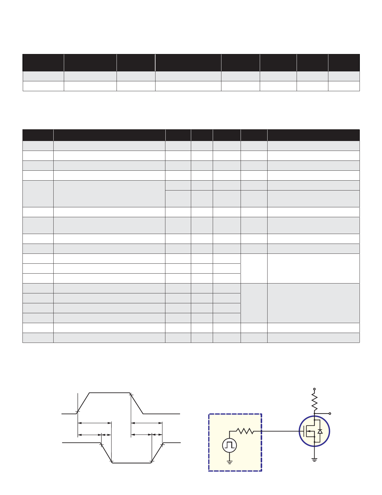
Switching Waveforms and Test Circuit
0V
INPUT
-10V
10%
VDD
OUTPUT
0V
t(ON)
td(ON)
tr
10%
90%
90%
t(OFF)
td(OFF)
tF
10%
90%
PULSE
GENERATOR
RGEN
INPUT
VDD
RL
OUTPUT
D.U.T.
2
Share Link: 