DG408L(2016) Ver la hoja de datos (PDF) - Vishay Semiconductors
Número de pieza
componentes Descripción
Fabricante
DG408L Datasheet PDF : 16 Pages
| |||
www.vishay.com
DG408L, DG409L
Vishay Siliconix
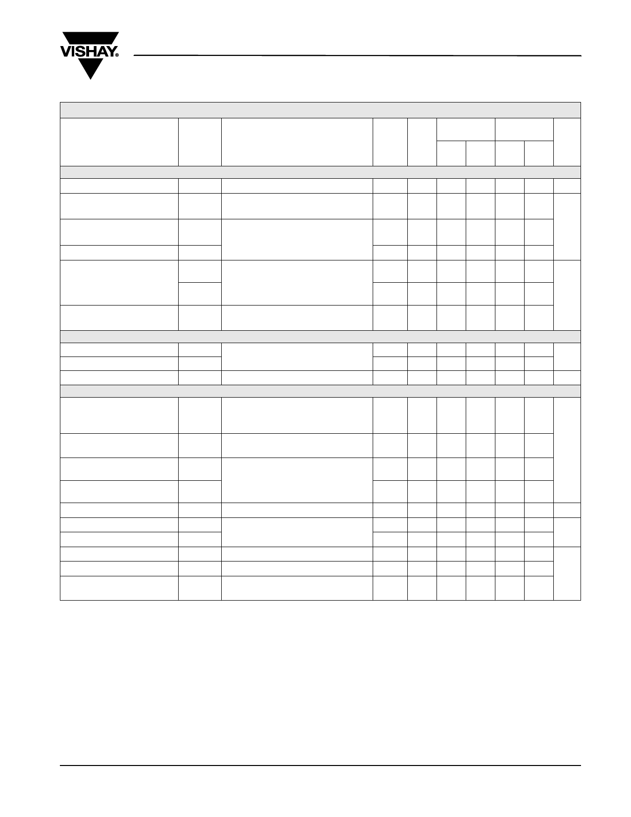
SPECIFICATIONS (Single Supply 5 V)
PARAMETER
Analog Switch
Analog Signal Range e
Drain-Source
On-Resistance
RDS(on) Matching Between
Channels g
On-Resistance Flatness i
Switch Off Leakage
Current a
SYMBOL
TEST CONDITIONS
UNLESS OTHERWISE
SPECIFIED
V+ = 5 V, ± 10 %, V- = 0 V
VEN = 0.6 V or 2.4 V f
TEMP. b
VANALOG
RDS(on)
V+ = 4.5 V, VD or VS = 1 V or 3.5 V,
IS = 5 mA
Full
Room
Full
RDS
RFLAT(on)
IS(off)
ID(off)
V+ = 4.5 V, VD = 1 V or 3.5 V,
IS = 5 mA
V+ = 5.5 V, VS = 1 V or 4 V,
VD = 4 V or 1 V
Room
Room
Room
Full
Room
Full
TYP. d
-
35
-
1.5
-
-
-
-
-
A SUFFIX
D SUFFIX
-55 °C to +125 °C -40 °C to +85 °C
MIN. c MAX. c MIN. c MAX. c
0
5
0
5
-
49
-
40
-
62
-
62
-
3
-
3
-
4
-
4
-1
1
-1
1
-15
15
-10
10
-1
1
-1
1
-15
15
-10
10
UNIT
V
nA
Channel On Leakage
Current a
ID(on)
V+ = 5.5 V, VD = VS = 1 V or 4 V, Room
sequence each switch on
Full
-
-
-1
1
-1
1
-15
15
-10
10
Digital Control
Logic High Input Voltage
VINH
V+ = 5 V
Full
Logic Low Input Voltage
VINL
Full
Input Current a
IIN
VAX = VEN = 2.4 V or 0.6 V
Full
Dynamic Characteristics
-
2.4
-
2.4
-
V
-
-
0.6
-
0.6
-
-1.5
1.5
-1
1
μA
Transition Time e
VS1 = 3.5 V, VS8 = 0 V, (DG408L) Room
44
tTRANS VS1b = 3.5 V, VS4b = 0 V, (DG409L)
see figure 2
Full
-
-
125
-
125
-
138
-
135
Break-Before-Make Time e tOPEN
VS(all) = VDA = 3.5 V,
Room 17
1
-
1
-
see figure 4
Full
-
-
-
-
-
ns
Room 43
-
60
-
60
Enable Turn-On Time e
tON(EN) VAX = 0 V, VS1 = 3.5 V (DG408L)
Full
-
-
70
-
65
Enable Turn-Off Time e
tOFF(EN)
VAX = 0 V, VS1b = 3.5 V (DG409L)
see figure 3
Room
Full
26
-
-
-
45
60
-
-
45
50
Charge Injection e
Q
CL = 1 nF, RGEN = 0 ,
VGEN = 0 V
Room
-1
-
-
-
-
pC
Off Isolation e, h
Crosstalk e
OIRR
Room -70
-
-
-
-
XTALK
f = 100 kHz, RL = 1 k
Room -80
-
-
-
dB
-
Source Off Capacitance e CS(off) f = 1 MHz, VS = 0 V, VEN = 0 V Room
8
-
-
-
-
Drain Off Capacitance e
CD(off) f = 1 MHz, VD = 0 V, VEN = 0 V Room
21
-
-
-
-
pF
Drain On Capacitance e
CD(on) f = 1 MHz, VD = 0 V, VEN = 2.4 V Room
32
-
-
-
-
Notes
a. Leakage parameters are guaranteed by worst case test condition and not subject to production test.
b. Room = 25 °C, full = as determined by the operating temperature suffix.
c. The algebraic convention whereby the most negative value is a minimum and the most positive a maximum, is used in this data sheet.
d. Typical values are for DESIGN AID ONLY, not guaranteed nor subject to production testing.
e. Guaranteed by design, not subject to production test.
f. VIN = input voltage to perform proper function.
g. RDS(on) = RDS(on) max. - RDS(on) min.
h. Worst case isolation occurs on channel 4 do to proximity to the drain pin.
i. RDS(on) flatness is measured as the difference between the minimum and maximum measured values across a defined Analog signal.
S16-0276-Rev. J, 22-Feb-16
5
Document Number: 71342
For technical questions, contact: analogswitchsupport@vishay.com
THIS DOCUMENT IS SUBJECT TO CHANGE WITHOUT NOTICE. THE PRODUCTS DESCRIBED HEREIN AND THIS DOCUMENT
ARE SUBJECT TO SPECIFIC DISCLAIMERS, SET FORTH AT www.vishay.com/doc?91000
Share Link: 