NX29F010 Ver la hoja de datos (PDF) - NexFlash -> Winbond Electronics
Número de pieza
componentes Descripción
Fabricante
NX29F010
NexFlash -> Winbond Electronics

NX29F010 Datasheet PDF : 25 Pages
| |||
NX29F010
Executing the Erase Command Sequence invokes the
Embedded Erase Algorithm, an internal algorithm that
automatically pre-programs the array to all zeros (if it is not
already programmed) before executing the erase operation.
During erase, the device automatically times the erase
pulse widths and verifies proper cell margin during erase.
By reading the DQ7 (Data Polling) and DQ6 (toggle) status
bits, the host system can detect whether a program or erase
operation is complete. After completion, the device is ready
to read array data or accept another command.
The sector erase architecture is designed to allow memory
sectors to be erased and reprogrammed without affecting
the data contents of other sectors. The device is erased
before it is shipped to customers.
The hardware data protection includes a low Vcc detector
that automatically inhibits write operations during power
transitions. The hardware sector protection feature will
disable both program and erase operations in any combina-
tion of the sectors of memory, and is implemented using
standard EPROM programming algorithm.
The device electrically erases all bits within a sector
simultaneously via Fowler-Nordheim tunneling. Data are
programmed one byte at a time using the EPROM program-
ming algorithm of hot electron injection.
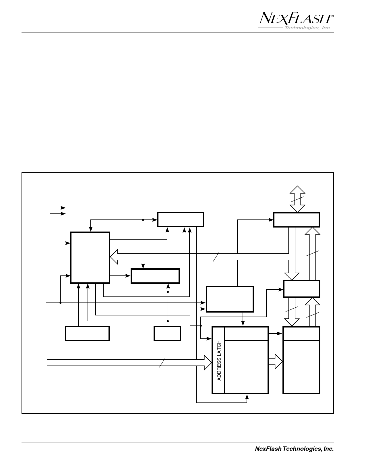
VCC
GND
WE
CE
OE
A0-A16
STATE
CONTROL
COMMAND
REGISTER
VCC
DETECTOR
ERASE VOLTAGE
GENERATOR
DQ7-DQ0
8
INPUT/OUTPUT
BUFFERS
PGM VOLTAGE
GENERATOR
STB
TIMER
8
8
8
STB
CHIP ENABLE/
OUTPUT ENABLE
LOGIC
DATA
LATCH
8
8
Y-DECODER
Y-GATING
X-DECODER
CELL
MATRIX
Figure 1. NX29F010 Block Diagram
2
NexFlash Technologies, Inc.
NXPF001F-0600
06/22/00 ©
Share Link: