NX29F010-45PL Ver la hoja de datos (PDF) - NexFlash -> Winbond Electronics
Número de pieza
componentes Descripción
Fabricante
NX29F010-45PL
NexFlash -> Winbond Electronics

NX29F010-45PL Datasheet PDF : 25 Pages
| |||
NX29F010
DQ6: Toggle Bit I
Toggle Bit I on DQ6 indicates whether an Embedded
Program or Erase algorithm is in progress or complete.
Toggle Bit I may be read at any address, and is valid after
the rising edge of the final WE pulse in the command
sequence (prior to the program or erase operation), and
during the sector erase time-out.
During an Embedded Program or Erase algorithm operation,
successive read cycles to any address cause DQ6 to
toggle. (The system may use either OE or CE to control the
read cycles.) When the operation is complete, DQ6 stops
toggling.
After an erase command sequence is written, if all sectors
selected for erasing are protected, DQ6 toggles for approxi-
mately 100 µs, then returns to reading array data. If not all
selected sectors are protected, the Embedded Erase algo-
rithm erases the unprotected sectors, and ignores the
selected sectors that are protected.
If a program address falls within a protected sector, DQ6
toggles for approximately 2 µs after the program command
sequence is written, then returns to reading array data.
The Write Operation Status table shows the outputs for
Toggle Bit I on DQ6. Refer to Figure 8 for the toggle bit
algorithm, and to the Toggle Bit Timings figure in the "AC
Characteristics" section for the timing diagram.
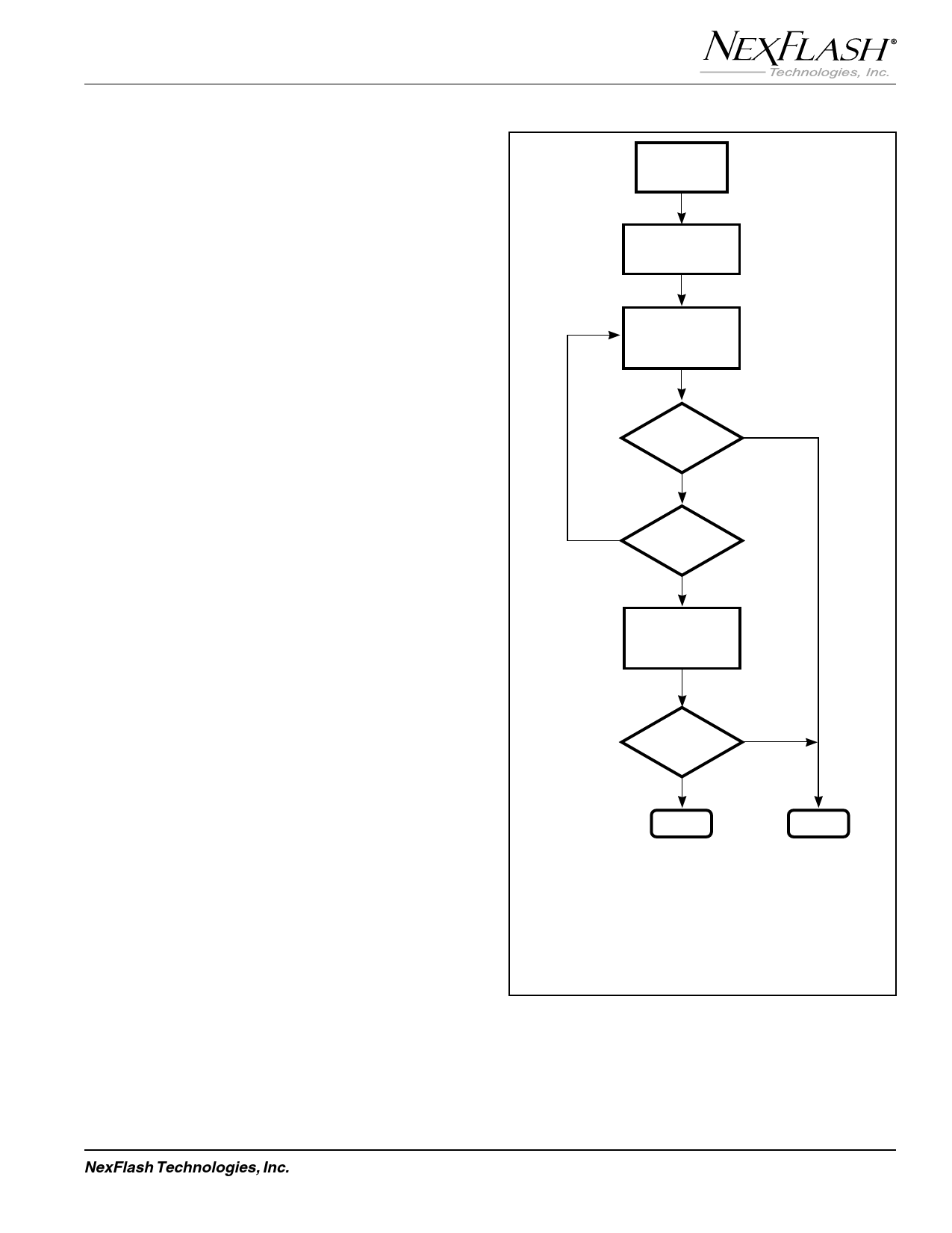
Reading Toggle Bit DQ6
Refer to Figure 8 for the following discussion. Whenever the
system initially begins reading toggle bit status, it must read
DQ7-DQ0 at least twice in a row to determine whether a
toggle bit is toggling.
Typically, a system would note and store the value of the
toggle bit after the first read. After the second read, the
system would compare the new value of the toggle bit with
the first. If the toggle bit is not toggling, the device has
completed the program or erase operation. The system can
read array data on DQ7-DQ0 on the following read cycle.
START
ADDR = VA
READ DQ7-DQ0(1)
OLD_DQ6 < DQ6
ADDR = VA
READ DQ7-DQ0
NEW_DQ6 < DQ6
NEW_DQ6 =
OLD_DQ6?
NO
YES
NO
DQ5 = 1?
YES
OLD_DQ6 < DQ6
ADDR = VA
READ DQ7-DQ0
NEW_DQ6 < DQ6
NEW_DQ6 =
OLD_DQ6?
NO
FAIL
YES
PASS
Notes:
1. Read toggle bit twice to determine whether or not it is
toggling. See text.
2. Recheck toggle bit because it may stop toggling as
DQ5 changes to '1'. See text.
3. VA = Valid Address.
Figure 8. Toggle Bit Algorithm
NexFlash Technologies, Inc.
11
NXPF001F-0600
06/22/00 ©
Share Link: