CY7C421-20JXI Ver la hoja de datos (PDF) - Cypress Semiconductor
NГәmero de pieza
componentes DescripciГіn
Fabricante
CY7C421-20JXI Datasheet PDF : 21 Pages
| |||
CY7C421
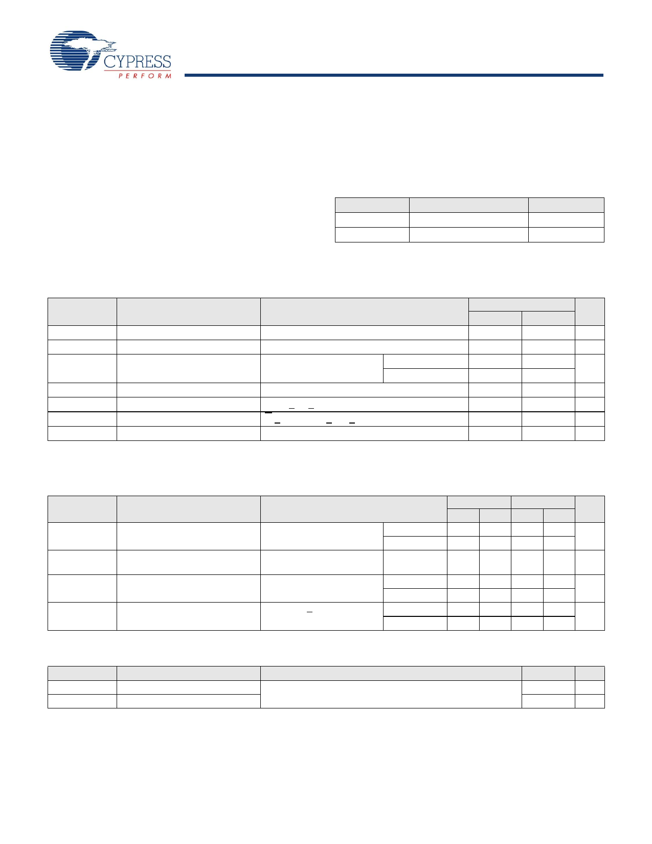
Maximum Ratings
Exceeding maximum ratings may impair the useful life of the
device. These user guidelines are not tested.[1]
Storage Temperature ............................... вҖ“65 В°C to +150 В°C
Ambient Temperature
with Power Applied .................................. вҖ“55 В°C to +125 В°C
Supply Voltage to Ground Potential .............вҖ“0.5 V to +7.0 V
DC Voltage Applied to Outputs
in High Z State .............................................вҖ“0.5 V to +7.0 V
DC Input Voltage .........................................вҖ“0.5 V to +7.0 V
Power Dissipation ........................................................ 1.0 W
Output Current, into Outputs (LOW) ........................... 20 mA
Static Discharge Voltage
(per MILвҖ“STDвҖ“883, Method 3015) ......................... > 2000 V
Latch Up Current ................................................... > 200 mA
Operating Range
Range
Commercial
Industrial
Ambient Temperature[2]
0 В°C to +70 В°C
вҖ“40 В°C to +85 В°C
VCC
5 V пӮұ 10%
5 V пӮұ 10%
Electrical Characteristics
Over the Operating Range
Parameter
VOH
VOL
VIH
VIL
IIX
IOZ
IOS
Description
Output HIGH Voltage
Output LOW Voltage
Input HIGH Voltage
Input LOW Voltage
Input Leakage Current
Output Leakage Current
Output Short Circuit Current [4]
Test Conditions
VCC = Min, IOH = вҖ“2.0 mA
VCC = Min, IOL = 8.0 mA
Commercial
Industrial
GND < VI < VCC
R > VIH, GND < VO < VCC
VCC = Max, VOUT = GND
All Speed Grades
Min
Max
2.4
вҖ“
вҖ“
0.4
2.0
VCC
2.2
VCC
[3]
0.8
вҖ“10
+10
вҖ“10
+10
вҖ“
вҖ“90
Unit
V
V
V
V
пҒӯA
пҒӯA
mA
Electrical Characteristics
Over the Operating Range
Parameter
ICC
Description
Operating Current
ICC1
Operating Current
ISB1
Standby Current
ISB2
Power Down Current
Test Conditions
VCC = Max, IOUT = 0 mA,
f = fMAX
VCC = Max, IOUT = 0 mA,
f = 20 MHz
All Inputs = VIH Min
All Inputs > VCC вҖ“ 0.2 V
Commercial
Industrial
Commercial
Commercial
Industrial
Commercial
Industrial
-15
Min Max
вҖ“
65
вҖ“ 100
вҖ“
35
-20
Min Max
вҖ“
55
вҖ“
90
вҖ“
35
Unit
mA
mA
вҖ“
10
вҖ“
10 mA
вҖ“
15
вҖ“
15
вҖ“
5
вҖ“
5 mA
вҖ“
8
вҖ“
8
Capacitance
Parameter [5]
Description
CIN
COUT
Input Capacitance
Output Capacitance
Test Conditions
TA = 25 В°C, f = 1 MHz, VCC = 4.5 V
Max Unit
6
pF
6
pF
Notes
1. Single Power Supply: The voltage on any input or I/O pin cannot exceed the power pin during power up.
2. TA is the вҖңinstant onвҖқ case temperature.
3. VIL(Min) = вҖ“2.0 V for pulse durations of less than 20 ns.
4. For test purposes, not more than one output at a time should be shorted. Short circuit test duration should not exceed 30 seconds.
5. Tested initially and after any design or process changes that may affect these parameters.
Document Number: 38-06001 Rev. *H
Page 6 of 21
Share Link: 