7C408A-15 Ver la hoja de datos (PDF) - Cypress Semiconductor
Número de pieza
componentes Descripción
Fabricante
7C408A-15 Datasheet PDF : 16 Pages
| |||
CY7C408A
CY7C409A
Possible Minimum Pulse Width Violation at the Boundary
Conditions
If the handshaking signals IR and OR are not properly used to
generate the SI and SO signals, it is possible to violate the
minimum (effective) SI and SO positive pulse widths at the full
and empty boundaries.
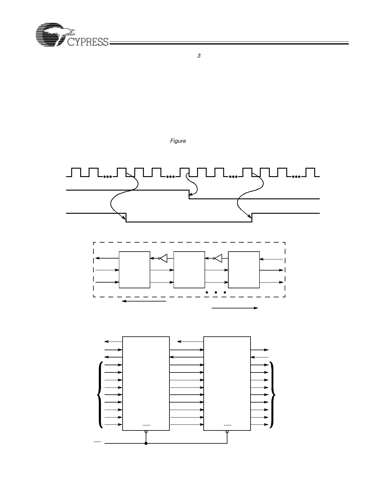
Cascading the 7C408/9A-35 Above 25 MHz
First, the capacity of N cascaded FIFOs is decreased from N
× 64 to (N × 63) + 1.
If cascaded FIFOs are to be operated with an external clock
rate greater than 25 MHz, the interface IR signal must be in-
verted before being fed back to the interface SO pin (Figure
3). Two things should be noted when this configuration is im-
plemented.
Secondly, the frequency at the cascade interface is less than
the 35 MHz rate at which the external clocks may operate.
Therefore, the first device has its data shifted in faster than it
is shifted out, and eventually this device becomes momentarily
full. When this occurs, the maximum sustainable external
clock frequency changes from 35 MHz to the cascade inter-
face frequency.[28]
When data packets[29] are transmitted, this phenomenon does
not occur unless more than three FIFOs are depth cascaded.
For example, if two FIFOs are cascaded, a packet of 127 (=2
× 63 + 1) words may be shifted in at up to 35 MHz and then
the entire packet may be shifted out at up to 35 MHz.
FULL
64 63
56 55 54
32 31 30
9
8
7
EMPTY
1
SHIFT OUT
HF
AFE
C408A–18
Figure 2. Shifting Words Out.
IRX
SIX
DINX
A
IR
IR
SO
SI
SI
OR
DIN
B
IR
SO
SI
OR
C
IR
SO
SI
OR
1
2
N
UPSTREAM
DOWNSTREAM
Figure 3. Cascaded Configuration Above 25 MHz.
HF/AFE
SHIFT IN
INPUT READY
DATA IN
128 x 9 Configuration
HF/AFE
SI
OR
IR
SO
DI0
DO0
DI1
DO1
DI2
DO2
DI3
DO3
DI4
DO4
DI5
DO5
DI6
DO6
DI7
DO7
DI8 MR DO8
SI
OR
IR
SO
DI0
DO0
DI1
DO1
DI2
DO2
DI3
DO3
DI4
DO4
DI5
DO5
DI6
DO6
DI7
DO7
DI8 MR DO8
SOX
ORX
DOUTX
C408A–19
OUTPUT READY
SHIFT OUT
DATA OUT
MR
C408A–20
Figure 4. Cascaded Configuration at or below 25 MHz [22,23,24,25,26].
9
Share Link: 