CY7C185D-15VXC Ver la hoja de datos (PDF) - Cypress Semiconductor
Número de pieza
componentes Descripción
Fabricante
CY7C185D-15VXC Datasheet PDF : 10 Pages
| |||
PRELIMINARY
CY7C185D
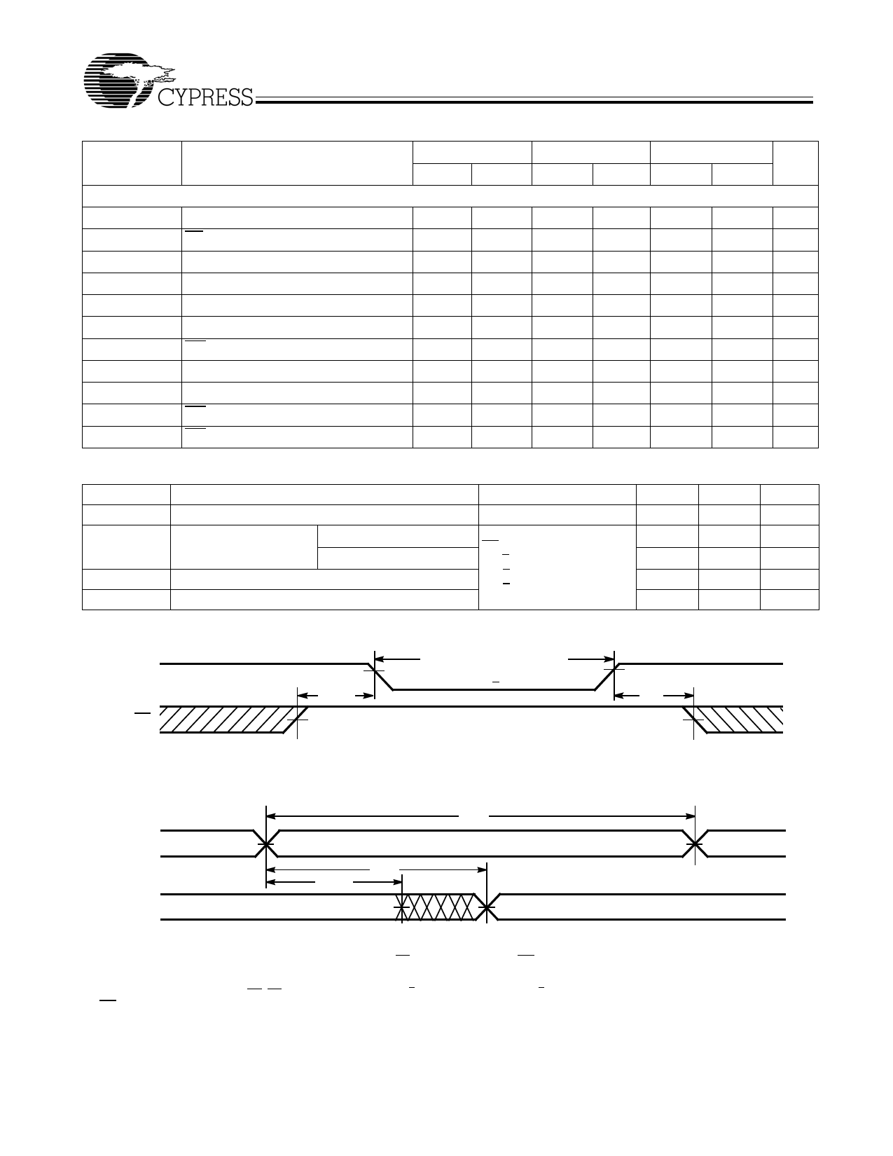
Switching Characteristics Over the Operating Range (continued)[6]
Parameter
Write Cycle[9]
tWC
tSCE1
tSCE2
tAW
tHA
tSA
tPWE
tSD
tHD
tHZWE
tLZWE
Description
Write Cycle Time
CE1 LOW to Write End
CE2 HIGH to Write End
Address Set-up to Write End
Address Hold from Write End
Address Set-up to Write Start
WE Pulse Width
Data Set-up to Write End
Data Hold from Write End
WE LOW to High Z[7]
WE HIGH to Low Z
7C185D-10
Min. Max.
7C185D-12
Min. Max.
10
12
8
10
8
10
7
10
0
0
0
0
7
10
6
7
0
0
6
6
3
3
Data Retention Characteristics (Over the Operating Range)
Parameter
VDR
ICCDR
tCDR [4]
tR[10]
Description
VCC for Data Retention
Data Retention Current Non-L, Com’l / Ind’l
L-Version Only
Chip Deselect to Data Retention Time
Operation Recovery Time
Conditions
VCC = VDR = 2.0V,
CE > VCC – 0.3V,
VIN > VCC – 0.3V or
VIN < 0.3V
Data Retention Waveform
7C185D-15
Min. Max.
15
12
12
12
0
0
12
8
0
7
3
Min.
2.0
0
tRC
Max.
3
1.2
Unit
ns
ns
ns
ns
ns
ns
ns
ns
ns
ns
ns
Unit
V
mA
mA
ns
ns
DATA RETENTION MODE
VCC
4.5V
VDR > 2V
4.5V
tCDR
tR
CE
Switching Waveforms
Read Cycle No.1[11,12]
tRC
ADDRESS
DATA OUT
tAA
tOHA
PREVIOUS DATA VALID
DATA VALID
Notes:
9. The internal write time of the memory is defined by the overlap of CE1 LOW, CE2 HIGH, and WE LOW. All 3 signals must be active to initiate a write and either
signal can terminate a write by going HIGH. The data input set-up and hold timing should be referenced to the rising edge of the signal that terminates the write.
10. Full device operation requires linear VCC ramp from VDR to VCC(min.) > 50 µs or stable at VCC(min.) > 50 µs.
11. Device is continuously selected. OE, CE1 = VIL. CE2 = VIH.
12. WE is HIGH for read cycle.
Document #: 38-05466 Rev. *C
Page 5 of 10
Share Link: 