HV430 Ver la hoja de datos (PDF) - Supertex Inc
Número de pieza
componentes Descripción
Fabricante
HV430 Datasheet PDF : 8 Pages
| |||
HV430
Pin Description
VPP1
Positive high voltage supply.
VPP2
Positive gate voltage supply. Generated by an internal linear regulator. A 25V, 100nF capacitor should be
connected between VPP2 and VPP1.
VNN1
Negative high voltage supply.
VNN2
Negative gate voltage supply. Generated by an internal linear regulator. A 25V, 100nF capacitor should be
connected between VNN2 and VNN1.
VDD
Logic supply voltage.
SGnd
Low voltage logic ground.
PGnd
High voltage power ground.
PIN
Logic control input. When mode is high, logic input high turns ON the external high voltage P-channel MOSFET.
Internally pulled low.
NIN
Logic control input. When mode is high, logic input high turns ON the external high voltage N-channel MOSFET.
Internally pulled low.
ENABLE
Logic enable input. Logic high enables IC. Internally pulled low.
MODE
Logic mode input. 0=single-control; 1=dual-control. When MODE is high, NIN and PIN independently control NOUT
and POUT, respectively. When MODE is low, NIN controls both outputs in a complementary manner.
(See Truth Table)
FAULT
Logic output. Fault is at logic low when either current limit sense pin, VPsen or VNsen, is activated. Remains
active until overcurrent condition clears or ENABLE=0 or RESET=0.
RESET
Power-on reset. A capacitor connected between this pin and ground determines the delay time between application
of VDD and when the device outputs are enabled. Low leakage tantalum recommended.
DEADBAND A resistor between this pin and ground sets the ‘break-before-make’ time between output transitions. Applicable
only in single-control mode. For minimum deadtime, a 5.6kΩ resistor to ground should be used. For dual-input
mode, tie to Vdd.
VPgate
Gate drive for external P-channel MOSFET.
VNgate
Gate drive for external N-channel MOSFET.
VPsen
Pulse by pulse over current sensing for P-Channel MOSFET.
VNsen
Pulse by pulse over current sensing for N-Channel MOSFET.
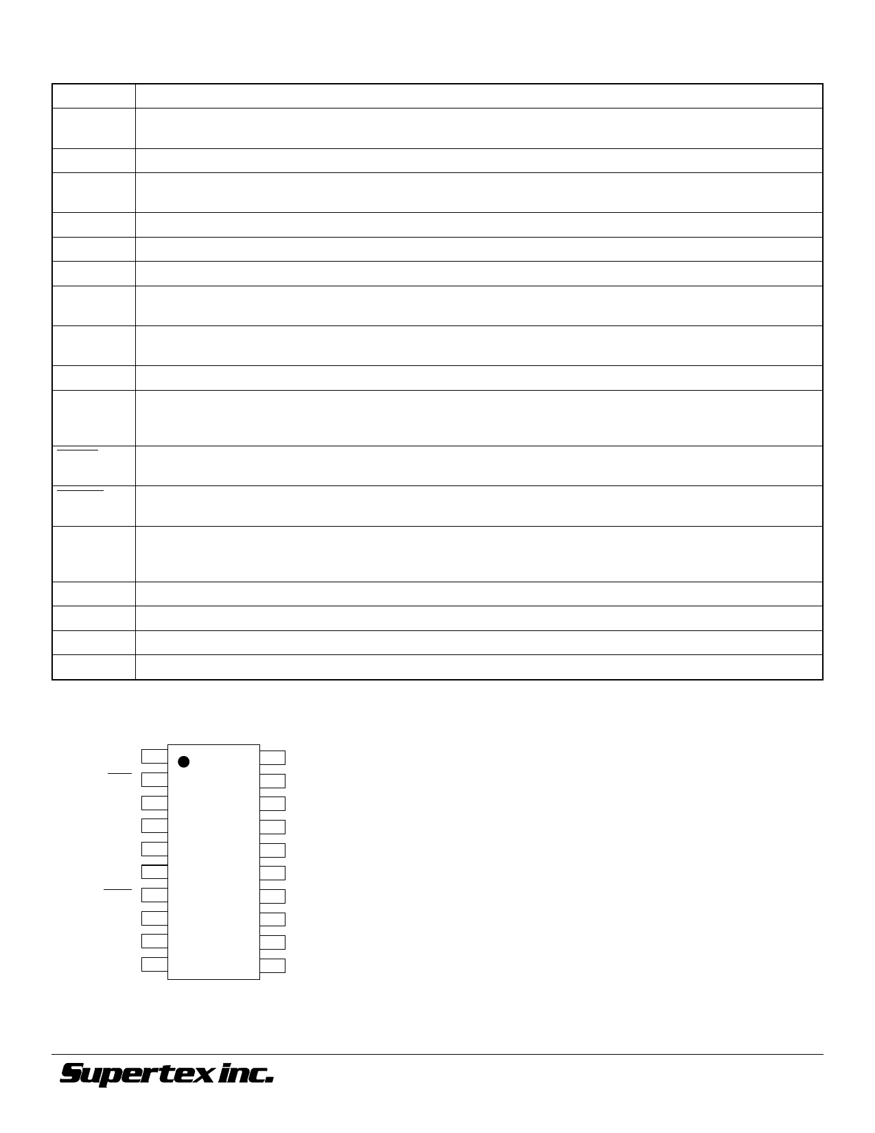
Pin Configuration
VDD
1
Fault 2
Mode 3
PIN
4
NIN
5
Enable 6
Reset 7
Deadband 8
SGND 9
PGND 10
20 VPP2
19 VPP1
18
VPSEN
17
VPGATE
16 N/C
15 N/C
14
VNGATE
13
VNSEN
12
VNN1
11
VNN2
top view
SOW 20
©2001 Supertex Inc. All rights reserved. Unauthorized use or reproduction prohibited.
8
12/13/010
1235 Bordeaux Drive, Sunnyvale, CA 94089
TEL: (408) 744-0100 • FAX: (408) 222-4895
www.supertex.com
Share Link: 