HV430 Ver la hoja de datos (PDF) - Supertex Inc
Número de pieza
componentes Descripción
Fabricante
HV430 Datasheet PDF : 8 Pages
| |||
Truth Table
Logic Inputs*
Output
NIN
PIN
mode
EN
RESET
External N-Channel External P-Channel
MOSFET
MOSFET
L
L
H
H
> Vreset(on)
L
H
H
H
> Vreset(on)
H
L
H
H
> Vreset(on)
H
H
H
H
> Vreset(on)
H
X
L
H
> Vreset(on)
OFF
OFF
ON
OFF
OFF
OFF
ON
OFF
OFF
ON
L
X
L
H
> Vreset(on)
X
X
X
L
X
ON
OFF
OFF
OFF
X
X
X
X
< Vreset(off)
OFF
OFF
* Unused logic inputs should be connected to VDD or GND.
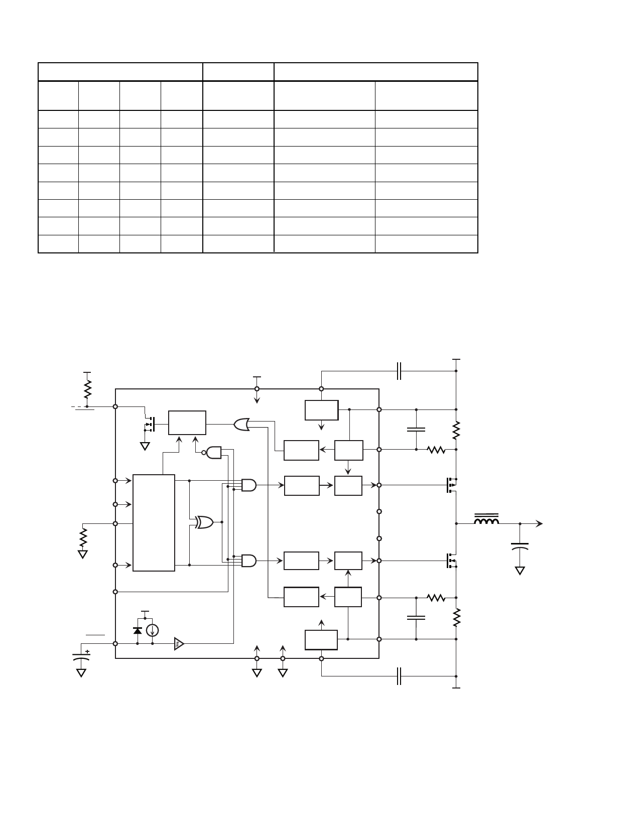
Block Diagram and Application Circuit
VDD
FAULT
De-glitcher
clk reset
PIN
MODE
DEADBAND
Control
Logic
NIN
ENABLE
RESET
VDD
10µA
+5V
VDD
VPP2
VPP2
Regulator
VPP1
Down
Translator
Current
Trip
VPSEN
Up
Translator
P
Driver
VPGATE
NC
Up
Translator
N
Driver
NC
VNGATE
Down
Translator
Current
Trip
VNSEN
SIG PWR
GND GND
VNN2
Regulator
VNN2
VNN1
VPP1
Rsense
Rsense
VNN1
Note: PIN, NIN, and ENABLE are internally pulled low. MODE is internally pulled high.
A Reset capacitor in the range of 1-10µF will yield a couple-second turn-on delay. Tantalum is recommended.
4
HV430
Ringer
Output
Share Link: 