CDP1824 Ver la hoja de datos (PDF) - Intersil
Número de pieza
componentes Descripción
Fabricante
CDP1824 Datasheet PDF : 6 Pages
| |||
CDP1824, CDP1824C
Static Electrical Specifications At TA = -40oC to +85oC, Except as Noted: (Continued)
CONDITIONS
LIMITS
CDP1824
CDP1824C
PARAMETER
VO
SYMBOL (V)
VIN
VDD
(NOTE 1)
(NOTE 1)
(V)
(V)
MIN
TYP
MAX MIN
TYP
MAX
Three-State Output
IOUT
0, 5
0, 5
5
-
± 0.2
±2.0
-
± 0.2
±2
Leakage Current
0, 10 0, 10
10
-
± 0.2
±2.0
-
-
-
Input Capacitance
CIN
-
-
-
-
5
7.5
-
5
7.5
Output Capacitance
COUT
-
-
-
-
10
15
-
10
15
NOTES:
1. Typical values are for TA = +25oC and nominal VDD.
2. Outputs open circuited; Cycle time = 1µs.
UNITS
µA
µA
pF
pF
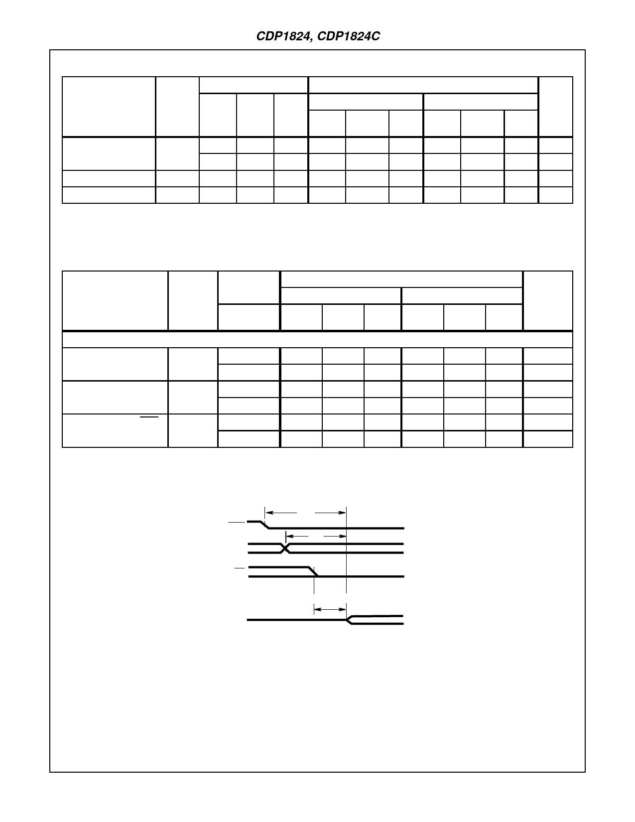
Dynamic Electrical Specifications at TA = -40oC to +85oC, VDD ±5%, Input tR, tF = 10ns, CL = 50pF, RL = 200kΩ; See Figure 1
TEST
CONDITIONS
LIMITS
CDP1824D, CDP1824E
CDP1824CD, CDP1824CE
PARAMETER
READ OPERATION
SYMBOL
VDD (V)
(NOTE 1) (NOTE 2)
(NOTE 1) (NOTE 2)
MIN
TYP
MAX
MIN
TYP
MAX
UNITS
Access Time From
Address Change
tAA
5
-
400
710
-
400
710
ns
10
-
200
320
-
-
-
ns
Access Time From
Chip Select
tDOA
5
10
-
300
710
-
300
710
ns
-
150
320
-
-
-
ns
Output Active From MRD
tAM
5
-
300
710
-
300
710
ns
10
-
150
320
-
-
-
ns
NOTES:
1. Time required by a limit device to allow for the indicated function.
2. Time required by a typical device to allow for the indicated function. Typical values are for TA = +25oC and nominal VDD.
MRD
MA
tAM
(NOTE 1)
tAA
CS
DATA OUT
(NOTE 1)
tDOA
HIGH IMPEDANCE
NOTES:
1. Minimum timing for valid data output longer times will initiate an earlier, but invalid output.
FIGURE 1. READ CYCLE TIMING DIAGRAMS
6-39
Share Link: 