CY7C1340A-66 Ver la hoja de datos (PDF) - Cypress Semiconductor
Número de pieza
componentes Descripción
Fabricante
CY7C1340A-66 Datasheet PDF : 12 Pages
| |||
CY7C1340A
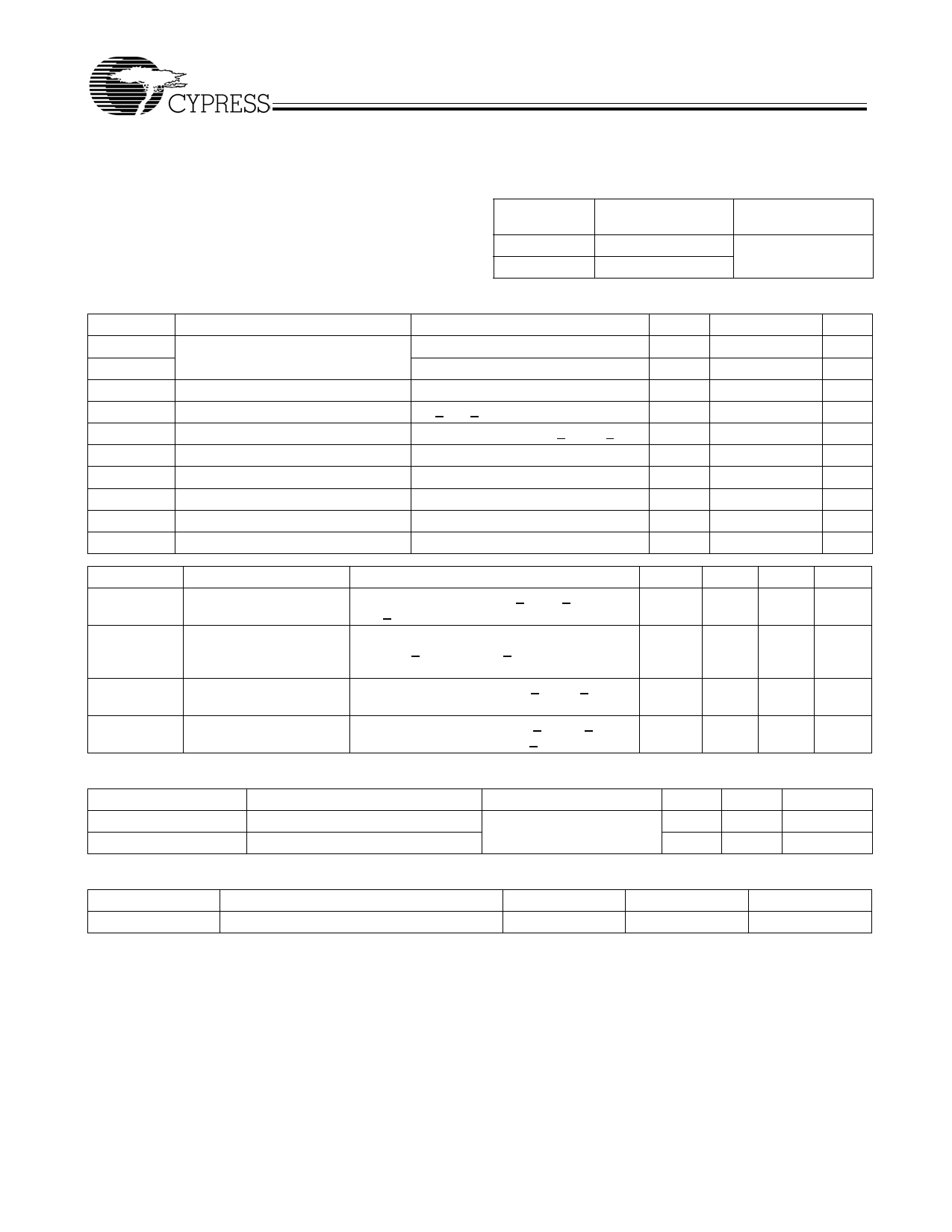
Maximum Ratings
(Above which the useful life may be impaired. For user guide-
lines, not tested.)
Voltage on VCC Supply Relative to VSS ......... –0.5V to +4.6V
VIN ...........................................................–0.5V to VCC+0.5V
Storage Temperature (plastic) .................... –55°C to +150°C
Junction Temperature ............................................... +150°C
Power Dissipation.......................................................... 1.0W
Short Circuit Output Current ........................................ 50 mA
Operating Range
Range
Commercial
Industrial
Ambient
Temperature[9]
0°C to +70°C
–40°C to +85°C
VDD[10,11]
3.3V −5%/+10%
Electrical Characteristics Over the Operating Range
Parameter
VIHD
VIH
VIl
ILI
ILO
VOH
VOL
VCC
VCCQ
VCCQ
Description
Input HIGH (Logic 1) Voltage[12, 13]
Input LOW (Logic 0) Voltage[12, 13]
Input Leakage Current[14]
Output Leakage Current
Output HIGH Voltage[12, 15]
Output LOW Voltage[12, 15]
Supply Voltage[12]
I/O Supply Voltage (3.3V I/O)[12]
I/O Supply Voltage (2.5V I/O)[12]
Test Conditions
Data Inputs (DQxx)
All Other Inputs
0V < VIN < VCC
Output(s) disabled, 0V < VOUT < VCC
IOH = –4.0 mA
IOL = 8.0 mA
Min.
2.0
2.0
–0.3
–2
–2
2.4
3.1
3.1
2.375
Max.
VCCQ + 0.3
4.6
0.8
2
2
0.4
3.6
3.6
VCC
Unit
V
V
V
µA
µA
V
V
V
V
Parameter
Description
Conditions
Typ.
-5
-7
Unit
ICC
Power Supply Current:
Operating[16, 17, 18]
Device selected; all inputs < VILor > VIH; cycle
time > tKC min.; VCC = Max.; outputs open
80
225 120 mA
ISB2
CMOS Standby[17, 18]
Device deselected; VCC = Max.;
0.2
2
2
mA
all inputs < VSS + 0.2 or >VCC – 0.2;
all inputs static; CLK frequency = 0
ISB3
TTL Standby[17, 18]
Device deselected; all inputs < VIL or > VIH; all 8
18
18
mA
inputs static; VCC = Max.; CLK frequency = 0
ISB4
Clock Running[17, 18]
Device deselected; all inputs < VIL or > VIH;
12
30
20
mA
VCC = Max.; CLK cycle time > tKC min.
Capacitance[19]
Parameter
CI
CO
Description
Input Capacitance
Input/Output Capacitance (DQ)
Test Conditions
TA = 25°C, f = 1 MHz,
VCC = 3.3V
Typ. Max.
Unit
3
4
pF
6
7
pF
Capacitance Derating[20]
Parameter
∆ tKQ
Description
Clock to Output Valid
Typ.
0.016
Max.
Notes:
9. TA is the case temperature.
10. Please refer to waveform (d).
11. Power supply ramp-up should be monotonic.
12. All voltages referenced to VSS (GND).
13. Overshoot: VIH ≤ +6.0V for t ≤ tKC /2.
Undershoot: VIL ≤ –2.0V for t ≤ tKC /2.
14. MODE pin has an internal pull-up and ZZ pin has an internal pull-down. These two pins exhibit an input leakage current of ±30 µA.
15. AC I/O curves are available upon request.
16. ICC is given with no output current. ICC increases with greater output loading and faster cycle times.
17. “Device Deselected” means the device is in power-down mode as defined in the truth table. “Device Selected” means the device is active.
18. Typical values are measured at 3.3V, 25°C, and 8.5-ns cycle time.
19. This parameter is sampled.
20. Capacitance derating applies to capacitance different from the load capacitance shown in AC Test Loads for 3.3V or 2.5V I/O.
Unit
ns/pF
Document #: 38-05153 Rev. *C
Page 6 of 12
Share Link: 