CY7C1212F Ver la hoja de datos (PDF) - Cypress Semiconductor
Número de pieza
componentes Descripción
Fabricante
CY7C1212F Datasheet PDF : 15 Pages
| |||
CY7C1212F
Thermal Resistance[10]
Parameter
ΘJA
ΘJC
Description
Thermal Resistance
(Junction to Ambient)
Thermal Resistance
(Junction to Case)
Test Conditions
Test conditions follow standard test methods and
procedures for measuring thermal impedance, per
EIA/JESD51
TQFP
Package
41.83
Unit
°C/W
9.99
°C/W
Capacitance[10]
Parameter
CIN
CCLK
CI/O
Description
Input Capacitance
Clock Input Capacitance
Input/Output Capacitance
Test Conditions
TA = 25°C, f = 1 MHz,
VDD = 3.3V.
VDDQ = 3.3V
Max. Unit
5 pF
5 pF
5 pF
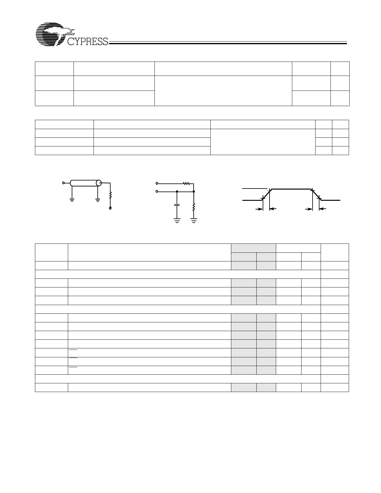
AC Test Loads and Waveforms
3.3V I/O Test Load
OUTPUT
Z0 = 50Ω
3.3V
OUTPUT
RL = 50Ω
5 pF
VL = 1.5V
(a)
INCLUDING
JIG AND
SCOPE
R = 317Ω
R = 351Ω
VDDQ
GND
ALL INPUT PULSES
10%
90%
≤ 1 ns
90%
10%
≤ 1 ns
(b)
(c)
Switching Characteristics Over the Operating Range[11, 12]
166 MHz
133 MHz
Parameter
Description
tPOWER
VDD(Typical) to the First Access[13]
Clock
Min. Max Min. Max Unit
1
1
ms
tCYC
Clock Cycle Time
tCH
Clock HIGH
tCL
Clock LOW
Output Times
6.0
7.5
ns
2.5
3.0
ns
2.5
3.0
ns
tCO
Data Output Valid after CLK Rise
tDOH
tCLZ
tCHZ
Data Output Hold after CLK Rise
Clock to Low-Z[14, 15, 16]
Clock to High-Z[14, 15, 16]
tOEV
tOELZ
tOEHZ
OE LOW to Output Valid
OE LOW to Output Low-Z[14, 15, 16]
OE HIGH to Output High-Z[14, 15, 16]
Set-up Times
3.5
4.0
ns
0.5
0.5
ns
0
0
ns
3.5
4.0
ns
3.5
4.5
ns
0
0
ns
3.5
4.0
ns
tAS
Address Set-up before CLK Rise
1.5
1.5
ns
Notes:
10. Tested initially and after any design or process change that may affect these parameters.
11. Timing reference level is 1.5V when VDDQ = 3.3V.
12. Test conditions shown in (a) of AC Test Loads unless otherwise tested.
13. This part has a voltage regulator internally; tPOWER is the time that the power needs to be supplied above VDD(minimum) initially before a Read or Write operation
can be initiated.
14. tCHZ, tCLZ,tOELZ, and tOEHZ are specified with AC test conditions shown in part (b) of AC Test Loads. Transition is measured ± 200 mV from steady-state voltage.
15. At any given voltage and temperature, tOEHZ is less than tOELZ and tCHZ is less than tCLZ to eliminate bus contention between SRAMs when sharing the same
data bus. These specifications do not imply a bus contention condition, but reflect parameters guaranteed over worst case user conditions. Device is designed
to achieve High-Z prior to Low-Z under the same system conditions
16. This parameter is sampled and not 100% tested.
Document #: 38-05423 Rev. *A
Page 8 of 15
Share Link: 