CY7C1212F Ver la hoja de datos (PDF) - Cypress Semiconductor
Número de pieza
componentes Descripción
Fabricante
CY7C1212F Datasheet PDF : 15 Pages
| |||
CY7C1212F
Single Write Accesses Initiated by ADSC
ADSC Write accesses are initiated when the following condi-
tions are satisfied: (1) ADSC is asserted LOW, (2) ADSP is
deserted HIGH, (3) CE1, CE2, CE3 are all asserted active, and
(4) the appropriate combination of the Write inputs (GW, BWE,
and BW[A:B]) are asserted active to conduct a Write to the
desired byte(s). ADSC-triggered Write accesses require a
single clock cycle to complete. The address presented to A is
loaded into the address register and the address
advancement logic while being delivered to the memory array.
The ADV input is ignored during this cycle. If a global Write is
conducted, the data presented to DQs is written into the corre-
sponding address location in the memory core. If a Byte Write
is conducted, only the selected bytes are written. Bytes not
selected during a Byte Write operation will remain unaltered.
A synchronous self-timed Write mechanism has been
provided to simplify the Write operations.
Because the CY7C1212F is a common I/O device, the Output
Enable (OE) must be deserted HIGH before presenting data
to the DQ inputs. Doing so will three-state the output drivers.
As a safety precaution, DQs are automatically three-stated
whenever a Write cycle is detected, regardless of the state of
OE.
Burst Sequences
The CY7C1212F provides a two-bit wraparound counter, fed
by A1, A0, that implements either an interleaved or linear burst
sequence. The interleaved burst sequence is designed specif-
ically to support Intel Pentium applications. The linear burst
sequence is designed to support processors that follow a
linear burst sequence. The burst sequence is user selectable
through the MODE input.
Asserting ADV LOW at clock rise will automatically increment
the burst counter to the next address in the burst sequence.
Both Read and Write burst operations are supported.
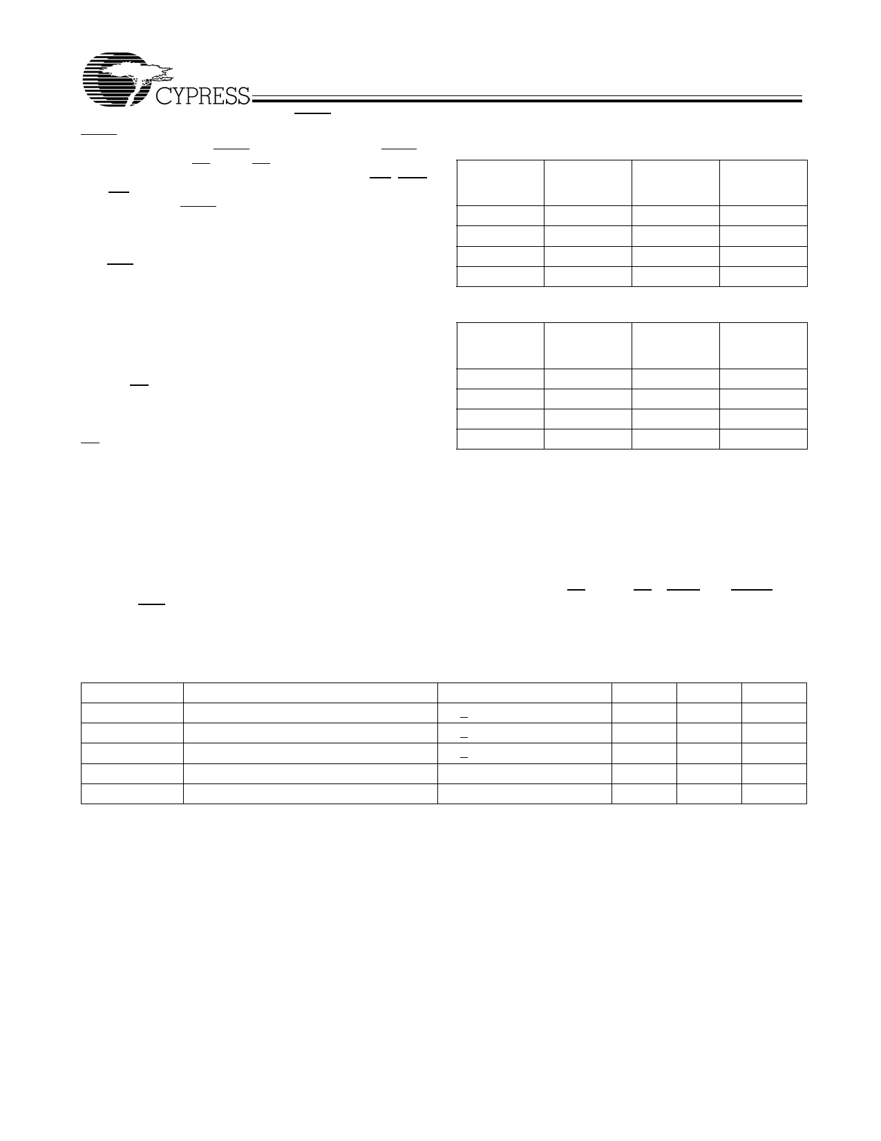
Interleaved Burst Address Table
(MODE = Floating or VDD)
First
Address
A1, A0
Second
Address
A1, A0
Third
Address
A1, A0
00
01
10
01
00
11
10
11
00
11
10
01
Fourth
Address
A1, A0
11
10
01
00
Linear Burst Address Table (MODE = GND)
First
Address
A1, A0
00
01
10
11
Second
Address
A1, A0
01
10
11
00
Third
Address
A1, A0
10
11
00
01
Fourth
Address
A1, A0
11
00
01
10
Sleep Mode
The ZZ input pin is an asynchronous input. Asserting ZZ
places the SRAM in a power conservation “sleep” mode. Two
clock cycles are required to enter into or exit from this “sleep”
mode. While in this mode, data integrity is guaranteed.
Accesses pending when entering the “sleep” mode are not
considered valid nor is the completion of the operation
guaranteed. The device must be deselected prior to entering
the “sleep” mode. CE1, CE2, CE3, ADSP, and ADSC must
remain inactive for the duration of tZZREC after the ZZ input
returns LOW.
ZZ Mode Electrical Characteristics
Parameter
IDDZZ
tZZS
tZZREC
tZZI
tRZZI
Description
Snooze mode standby current
Device operation to ZZ
ZZ recovery time
ZZ Active to snooze current
ZZ Inactive to exit snooze current
Test Conditions
ZZ > VDD – 0.2V
ZZ > VDD – 0.2V
ZZ < 0.2V
This parameter is sampled
This parameter is sampled
Min.
2tCYC
0
Max.
40
2tCYC
2tCYC
Unit
mA
ns
ns
ns
ns
Document #: 38-05423 Rev. *A
Page 5 of 15
Share Link: 