29F0408RPFI Ver la hoja de datos (PDF) - MAXWELL TECHNOLOGIES
Número de pieza
componentes Descripción
Fabricante
29F0408RPFI Datasheet PDF : 32 Pages
| |||
32 Megabit (4M x 8-Bit) Flash Memory
29F0408
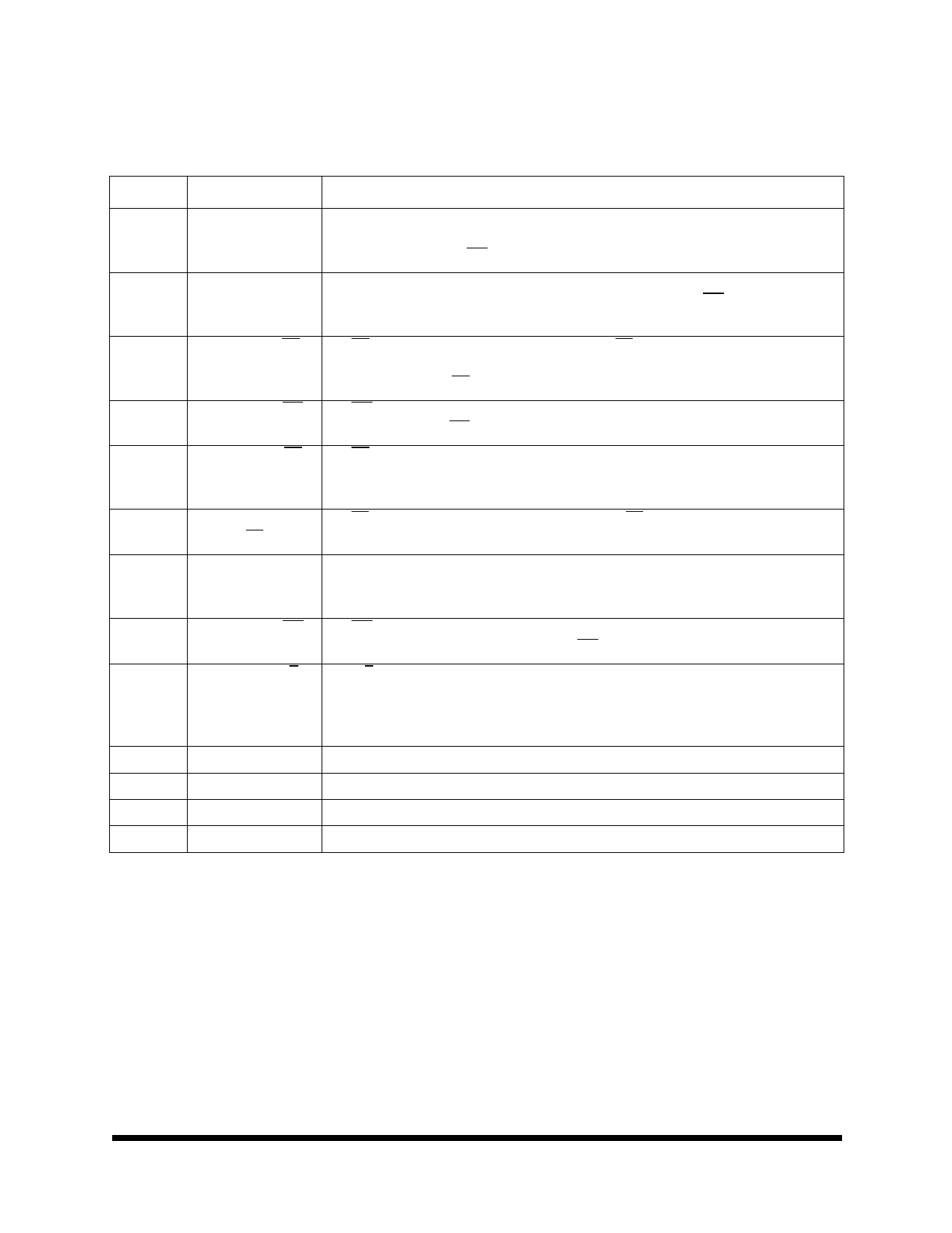
TABLE 1. PINOUT DESCRIPTION
PIN
SYMBOL
DESCRIPTION
2
Command Latch The CLE input controls the path activation for commands sent to the command register.
Enable (CLE) When active high, commands are latched into the command register through the I/O ports
on the rising edge of the WE signal.
3
Address Latch Enable The ALE input controls the path activation for address and input data to the internal
(ALE)
address/data register. Addresses are latched on the rising edge or WE with ALE high, and
input data is latched when ALE is low.
43
Chip Enable (CE) The CE input is the device selection control. When CE goes high during a read operation,
the device is returned to standby mode. However, when the device is in the busy state dur-
ing program or erase, CE high is ignored, and does not return the device to standby mode.
4
Write Enable (WE) The WE input controls writes to the I/O port. Commands, address and data are latched on
the rising edge of the WE pulse.
42
Read Enable (RE) The RE inputs is the serial data-out control, and when active drives the data onto the I/O
bus. Data is valid tREA after the falling edge of RE which also increments the internal column
address counter by one.
40
Spare Area Enable The SE input controls the spare area selection when SE is high, the device is deselected
(SE)
the spare area during Read1, Sequential data input and page Program.
18-21,
24-27
I/O Port: I/O0 ~ I/O7 The I/O pins are used to input command, address and data, and to output data during read
operations. The I/O pins float to High-Z when the chip is deselected or when the outputs are
disabled.
5
Write Protect (WP) The WP pin provides inadvertent write/erase protection during power transitions. The inter-
nal high voltage generator is reset when the WP pin is active low.
41
Read/Busy (R/B) The R/B output indicates the status of the device operation. When low, it indicates that a
program, erase or random read operation is in process and returns to high state upon com-
pletion. It is an open drain output and does not float to High-Z condition when the chip is
deselected or when outputs are disabled.
6-17, 28-39
NC
Not Connected
1, 22
VSS
Ground
44
VCC
Supply Voltage
23
VCCQ
Output Buffer Voltage
11.08.02 Rev 2
All data sheets are subject to change without notice 2
©2002 Maxwell Technologies
All rights reserved.
Share Link: 